Preparation method for center-wiring double-circle-arrangement single-IC (integrated circuit) chip packaging piece

A chip packaging and wiring technology, used in semiconductor/solid-state device manufacturing, electrical components, electrical solid-state devices, etc., can solve the problems of small number of pins, high cost of bonding wires, and long bonding wires.

Active Publication Date: 2015-06-17
TIANSHUI HUATIAN TECH +1
View PDF9 Cites 0 Cited by
  • Summary
  • Abstract
  • Description
  • Claims
  • Application Information

AI Technical Summary

Problems solved by technology

At present, the common quad flat no-lead package (QFN) single-sided packaging has fewer pins and long bonding wires, resulting in high bonding wire costs

Method used


Image

  • Preparation method for center-wiring double-circle-arrangement single-IC (integrated circuit) chip packaging piece
  • Preparation method for center-wiring double-circle-arrangement single-IC (integrated circuit) chip packaging piece
  • Preparation method for center-wiring double-circle-arrangement single-IC (integrated circuit) chip packaging piece

Examples


Embodiment 1

[0035] Step 1 thinning and dicing

[0036] The wafer is thinned to 180μm and diced by conventional methods, and the dicing feed speed is controlled at ≤10mm / s;

[0037] Step 2 Core

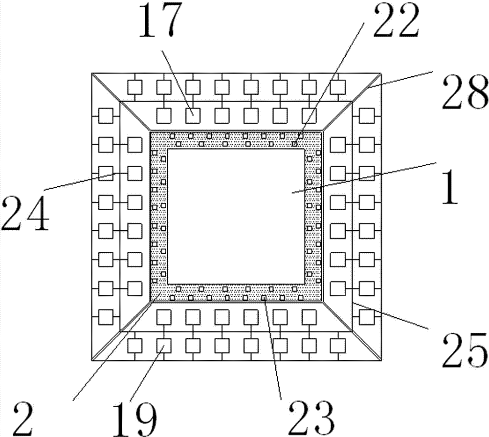
[0038] Take the lead frame carrier, fix the IC chip 4 that has been thinned and diced in step 1 on the double-circle lead frame carrier 1, and bake for 3 hours with the anti-separation layer baking technology, the baking temperature is 150°C, and use ESPEC and other exhaust gases. Unobstructed, the temperature difference is less than ± 3 ℃ oven.

[0039] Step 3 Pressure Welding

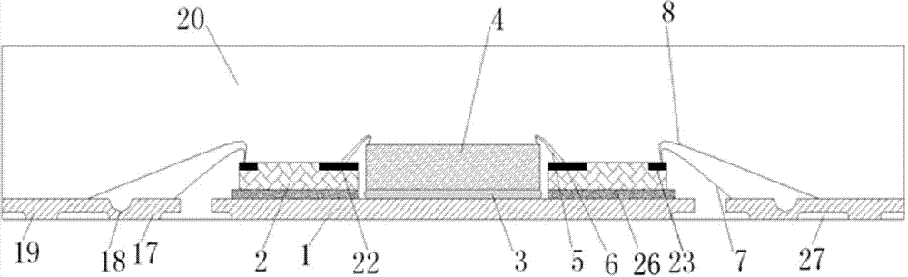
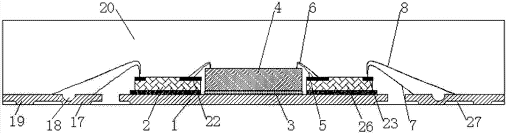
[0040] First place the semi-finished lead frame transfer box with the center wiring ring 2 glued to the IC chip 4 on the feeding table of the pressure welding machine, then fix the gold wire or copper spool on the pressure welding table, and start the automatic loading of the pressure welding machine material device, the finished lead frame transfer box automatically rises to the set position, pushes out a semi-finishe...

Embodiment 2

[0050] Step 1 thinning and dicing

[0051] The wafer is thinned to 210μm and diced by conventional methods, and the dicing feed speed is controlled at ≤10mm / s;

[0052] Step 2 Core

[0053] Take the lead frame carrier, fix the IC chip 4 that has been thinned and diced in step 1 on the double-circle lead frame carrier 1, and bake for 3 hours with the anti-separation layer baking technology, the baking temperature is 150°C, and use ESPEC and other exhaust gases. Unobstructed, the temperature difference is less than ± 3 ℃ oven.

[0054] Step 3 Pressure Welding

[0055] First place the semi-finished lead frame transfer box with the center wiring ring 2 glued to the IC chip 4 on the feeding table of the pressure welding machine, then fix the gold wire or copper spool on the pressure welding table, and start the automatic loading of the pressure welding machine The finished lead frame transfer box automatically rises to the set position, pushes out a semi-finished lead frame to t...

Embodiment 3

[0065] Step 1 thinning and dicing

[0066] The wafer is thinned to 210μm and diced by conventional methods, and the dicing feed speed is controlled at ≤10mm / s;

[0067] Step 2 Core

[0068] Take the lead frame carrier, fix the IC chip 4 that has been thinned and diced in step 1 on the double-circle lead frame carrier 1, and bake for 3 hours with the anti-separation layer baking technology, the baking temperature is 150°C, and use ESPEC and other exhaust gases. Unobstructed, the temperature difference is less than ± 3 ℃ oven.

[0069] Step 3 Pressure Welding

[0070] First place the semi-finished lead frame transfer box with the center wiring ring 2 glued to the IC chip 4 on the feeding table of the pressure welding machine, then fix the gold wire or copper spool on the pressure welding table, and start the automatic loading of the pressure welding machine The finished lead frame transfer box automatically rises to the set position, pushes out a semi-finished lead frame to t...


PUM


Abstract

The invention relates to a center-wiring double-circle-arrangement single-IC (integrated circuit) chip packaging piece and a preparation method of the packaging piece. An IC chip is adhered on a lead frame carrier, a center-wiring ring is arranged on the outer side of the IC chip, two circles of inner pins are arranged outside the center-wiring ring, an inner circle of pad and an outer circle of pad are arranged on the center-wiring ring, the inner circle of pad conducts routing with the pad of the IC chip, and the outer circle of pad conducts routing with the first inner pin and the second inner pin respectively. According to the invention, the center-wiring ring and salient points arranged in double circles are smartly combined, and the center-wiring ring is connected with or embedded in the lead frame carrier by high-strength glue, thereby enhancing the combination of plastic packaging material and the frame, reducing the thickness of the frame, preventing layering, and being favorable for improving the reliability of products. The two circles of pads on the center-wiring ring are connected with each other by a PCB (printed circuit board) design line and are connected with the inner pins by switching of the internal line of the center-wiring ring as the IC chip, thereby reducing the length of a bonding wire, and saving the cost of the bonding wire, especially the use cost of gold wires.

Description

technical field [0001] The invention relates to the technical field of electronic information automation component manufacturing, and relates to an IC chip package, specifically a single IC chip package with a central wiring double-circle arrangement, and also relates to a preparation method of the package. Background technique [0002] For a long time, limited by the etching template and etching process technology, QFN products have continued the single-turn lead frame mode developed in the 1990s. The integrated circuit packaging technology of QFN (Quad Flat No Lead Package) type double-circle array packaging is a new type of micro-shaped high-density packaging technology developed in recent years. Especially since 2006, the market demand has increased, which has promoted the QFN packaging technology. The rapid development of materials technology, manufacturing technology and packaging application technology have all made breakthroughs. At present, the common quad flat no-...

Claims


Application Information

Patent Timeline
Patent Type & Authority Patents(China)
IPC IPC(8): H01L23/495H01L21/60
CPCH01L2224/45144H01L2224/48091H01L2224/73265
Inventor 朱文辉郭小伟慕蔚李习周
Owner TIANSHUI HUATIAN TECH
Why Eureka
Try Eureka