Touch display panel

A touch display panel and substrate technology, applied in static indicators, optics, instruments, etc., can solve problems such as poor display brightness and achieve high aperture ratio

Active Publication Date: 2010-04-28
CENTURY DISPLAY (SHENZHEN) CO LTD
View PDF0 Cites 16 Cited by
  • Summary
  • Abstract
  • Description
  • Claims
  • Application Information

AI Technical Summary

Problems solved by technology

Therefore, the aperture ratio of the touch display panel 100 will be affected to a considerable extent, resulting in poor display brightness.

Method used


Image

  • Touch display panel
  • Touch display panel
  • Touch display panel

Examples


Embodiment Construction

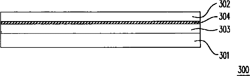
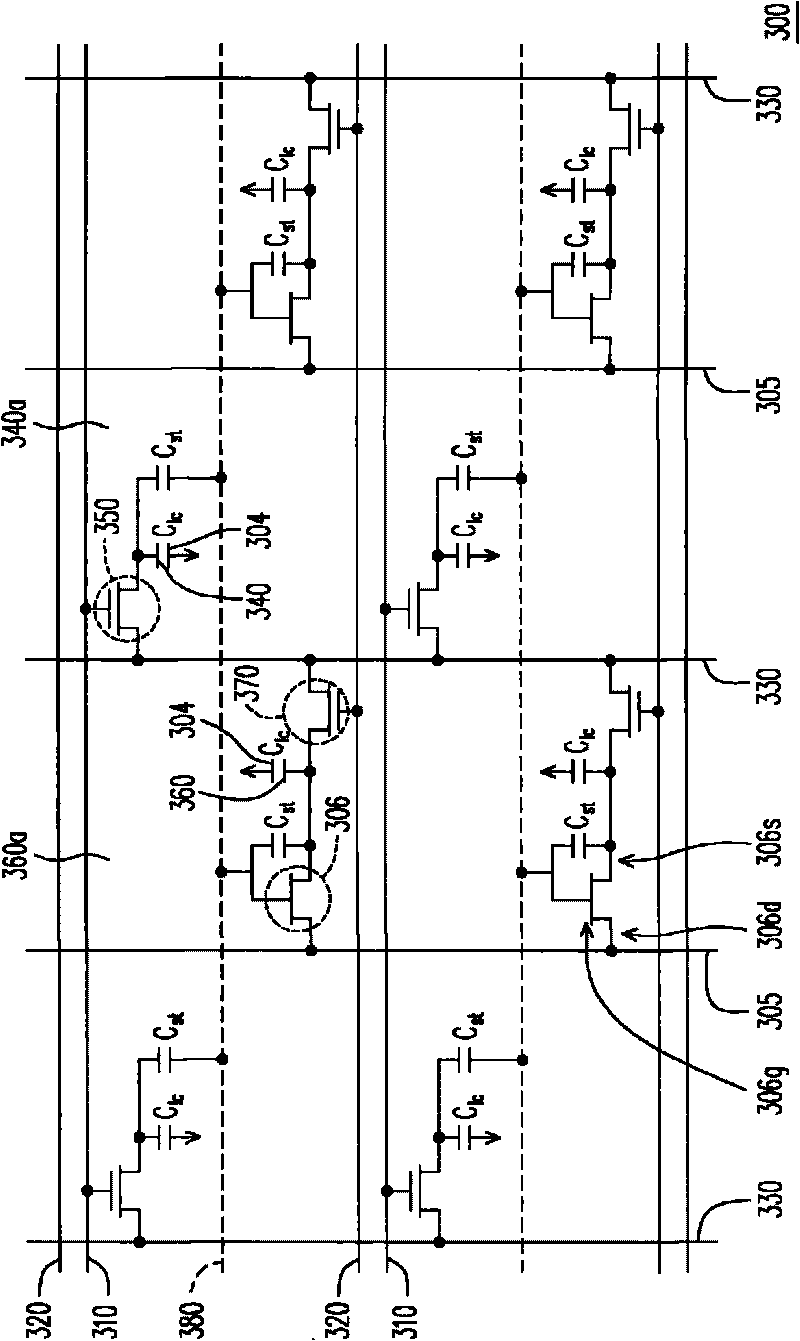
[0035] figure 2 It is a schematic side view of a touch display panel 300 according to an embodiment of the present invention. image 3 for figure 2 A schematic diagram of the circuit structure of the touch display panel 300 . Figure 4 for figure 2 A partial schematic diagram of the touch display panel 300 . Figure 5 for Figure 4 A schematic cross-sectional view of the touch display panel 300 along the line A-A'.

[0036] Please refer to figure 2 , image 3 , Figure 4 and Figure 5 The touch display panel 300 includes a first substrate 301 , a second substrate 302 and a display medium layer 303 . A plurality of first scan lines 310, a plurality of second scan lines 320, a plurality of data lines 330, a plurality of first pixel structures 340a, a plurality of second pixel structures 360a, and a plurality of common electrode lines are arranged on the first substrate 301 380 , multiple reading lines 305 , and multiple photosensitive thin film transistors 306 . I...


PUM


Abstract

The invention relates to a touch display panel, which comprises a first substrate, a second substrate and a display medium layer. The first substrate is provided with a plurality first scanning lines, a plurality of second scanning lines, a plurality of data lines, a plurality of first pixel structures, a plurality of second pixel structures, a plurality of common electrode wires, a plurality of reading lines and a plurality of photosensitive thin film transistors. The plurality of reading lines are arranged on the first substrate and each reading line is positioned between two adjacent data lines. The plurality of photosensitive thin film transistors are arranged on the first substrate, wherein each photosensitive thin film transistor is electrically connected with one of the common electrode wires, one of the reading lines and one of the first pixel structures; or each photosensitive thin film transistor is electrically connected with one of the common electrode wires, one of the reading lines and one of the second pixel structures.

Description

【Technical field】 [0001] The present invention relates to a touch display panel, and in particular to a touch display panel with high brightness. 【Background technique】 [0002] In recent years, with the rapid development and wide application of information technology, wireless communication and information home appliances, the operation interface of many information products has changed from the traditional keyboard or mouse to use touch panels as input devices. [0003] At present, the common touch display device is to assemble the touch panel and the display panel after the touch panel and the display panel are manufactured separately, so there are disadvantages such as high cost, heavy weight and low light transmittance. In order to improve the above shortcomings, the touch panel and the display panel are integrated into one panel to form a liquid crystal display panel with touch function. [0004] figure 1 It is a simple circuit schematic diagram of an existing touch ...

Claims


Application Information

Patent Timeline
Patent Type & Authority Applications(China)
IPC IPC(8): G02F1/133G02F1/1368G06F3/041
Inventor 李俊谊
Owner CENTURY DISPLAY (SHENZHEN) CO LTD
Why Eureka
Try Eureka