

Palladium-plated bonded copper wire and production method thereof
A technology for bonding copper wires and a manufacturing method, which is applied in the manufacture of semiconductor/solid-state devices, electrical components, electrical solid-state devices, etc., and can solve the problems of poor high temperature stability, easy surface oxidation, low hardness of electroplating layer and inability to resist friction, etc.
- Summary
- Abstract
- Description
- Claims
- Application Information
AI Technical Summary
Problems solved by technology
Method used
Image

Examples
Embodiment 1
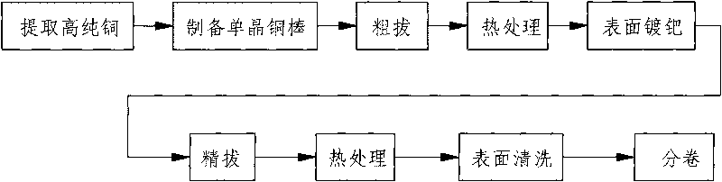
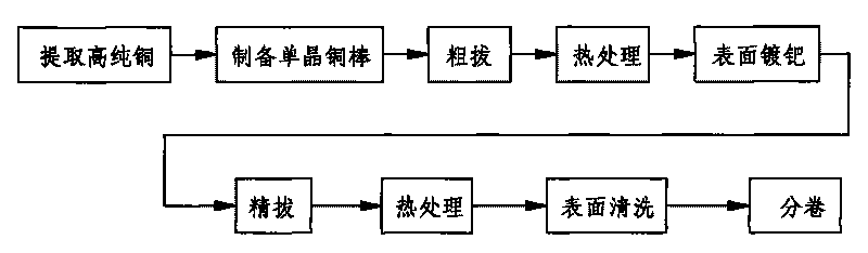
[0023] ① Extraction of high-purity copper: Dilute the copper nitrate solution with high-purity water at a ratio of 1:4 to prepare an electrolyte; use the national standard No. 1 pure copper as the anode to immerse in the electrolyte, and ensure that 95% of the volume ratio of pure copper is immersed in the electrolysis liquid; use high-purity copper foil as the cathode to immerse in the electrolyte, and also ensure that 95% of the volume ratio of high-purity copper foil is immersed in the electrolyte; input a direct current of 7-9V, 2.5-3.5A between the anode and the cathode, Maintain the temperature of the electrolyte not exceeding 60°C by replenishing fresh electrolyte; when the cathode accumulates high-purity copper with a purity greater than 99.9995%, replace the high-purity copper foil in time, and then clean and dry it for later use.
[0024] ②Preparation of single crystal copper rods: In a continuous casting room for horizontal continuous casting of metal single crystals...
Embodiment 2
[0033] Step 1. to step 4. are the same as in Embodiment 1.
[0034] ⑤Palladium plating on the surface: Apply conventional electroplating equipment and technology to the annealed Copper wire electroplating pure palladium anti-oxidation protective layer, the purity of palladium used for electroplating is required to be greater than 99.999%; the current density is 4-4.5A / dm 2 , the speed of copper wire is 4-5m / min, and the thickness of the coating is controlled at 3μm; the copper wire product after palladium plating is 8.92g / cm according to the density of pure copper 3 , The density of pure palladium is 12.0g / cm 3 In conversion, it can be known that the weight percentage of palladium is 8.19%, and the rest is copper.
[0035] ⑥Precise drawing: using conventional precision drawing equipment and technology, the aforementioned pure palladium anti-oxidation protective layer is electroplated The copper wire is precision drawn through multi-pass process palladium-coated copper bon...
PUM
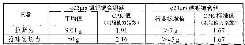
| Property | Measurement | Unit |
|---|---|---|
| Diameter | aaaaa | aaaaa |
| Density | aaaaa | aaaaa |
| Density | aaaaa | aaaaa |
Abstract
Description
Claims
Application Information