
Metal spring leaf in electronic product and connecting structure adopting same

A technology of metal reeds and electronic products, applied in the direction of connection, fixed connection, circuits, etc., can solve the problems of PCB board pad pull-up, metal reed bump deformation, PCB board scrapping, etc., to reduce bump deformation, reduce The amount of deformation and the effect of avoiding PCB scrap

Active Publication Date: 2010-05-12
ZTE CORP
View PDF0 Cites 11 Cited by
  • Summary
  • Abstract
  • Description
  • Claims
  • Application Information

AI Technical Summary

Problems solved by technology

In the application of this kind of metal reed, the metal reed often bumps and deforms, and sometimes the PCB pad is pulled up due to excessive force, resulting in the scrapping of the PCB

Method used


Image

  • Metal spring leaf in electronic product and connecting structure adopting same
  • Metal spring leaf in electronic product and connecting structure adopting same
  • Metal spring leaf in electronic product and connecting structure adopting same

Examples


Embodiment 1

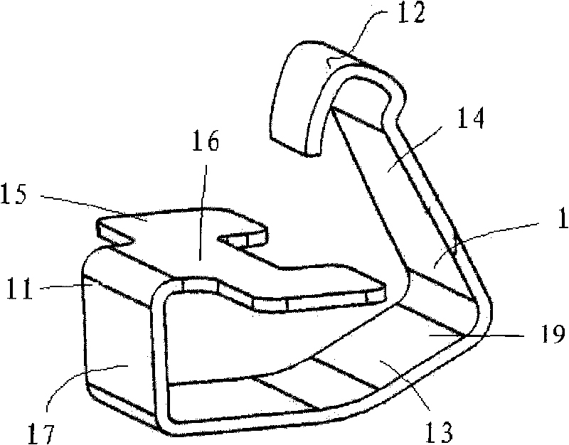
[0028] Such as figure 1 As shown, the metal reed 1 includes a reed body 19 with elastic bending, a contact end 12 and a welding end 11 . The reed body 19 includes a bent portion 13, a first supporting piece 14 is extended from one end of the bent portion 13, and a second supporting piece 17 is extended from the other end. In this embodiment, the bent portion 13 is approximately V-shaped. The first supporting piece portion 14 and the second supporting piece portion 17 are located on the same plane of the bent portion 13, and the first supporting piece portion 14 and the second supporting piece portion 17 have a certain angle, which can be 0° to 90°. In this embodiment, the included angle is 30 degrees. The contact end 12 is arranged at the end of the first support piece 14 , and the soldering end 11 is arranged at the end of the second support piece 17 . The welding end 11 is close to the middle of the reed body 19 , the contact end 12 is located at the upper part of the reed...

Embodiment 2

[0040] The difference from Embodiment 1 is that the shape of the bent portion 13 of the metal reed 1 of this embodiment is approximately L-shaped, such as Figure 4 As shown, the first supporting piece portion 14 and the second supporting piece portion 17 are respectively located on two surfaces of the bent portion 13 . In addition, pins 18 extending perpendicular to the side wing plate 15 are provided on both sides of the side wing plate 15 , and the pins 18 are used to assist in fixing the metal reed 1 to the PCB 2 . In this embodiment, the angle between the first support piece 14 and the second support piece 17 is 60 degrees. All the other structures are the same as in Example 1. The pins 18 , the side panels 15 , the welding platform 16 and the welding end 11 are integrally formed. The pins 18, the side panels 15 and the welding platform 16 are all flat pieces with smooth surfaces.

[0041] The structure in which the metal reed 1 of this embodiment is welded to the PCB ...


PUM


Abstract

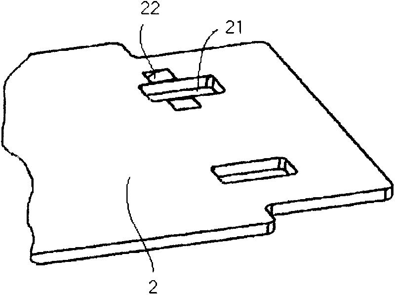
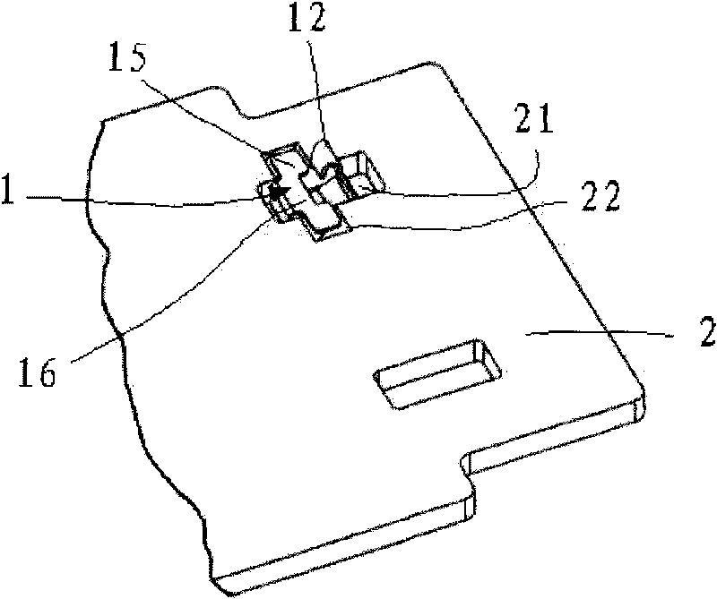
The invention provides a metal spring leaf in an electronic product and a connecting structure adopting the metal spring leaf, which comprises a metal spring leaf and a PCB. The metal spring leaf comprises a spring leaf body with an elastic back bending structure; a contact end and a welding end are arranged at both ends of the spring leaf body; the welding end is near to the middle part of the spring leaf body; a hole groove is arranged on the PCB; and the metal spring leaf is arranged in the hole groove and welded on the PCB bard through the welding end. As the metal spring leaf has the elastic back bending structure, and the welding end is arranged at the middle part of the elastic back bending structure, the dimension of the metal spring leaf is greatly reduced, and the deformation of the metal spring leaf is reduced. As the metal spring leaf is arranged in the hole groove on the PCB, the exposed part of the metal spring leaf is reduced; therefore, the metal spring leaf can be elastically compressed in the hole groove, and the probability of deformation failure caused by unexpected collision of the metal spring leaf is reduced.

Description

technical field [0001] The invention relates to a metal reed in an electronic product and a connection structure using the metal reed. Background technique [0002] Metal reeds are often used in electronic products such as mobile phones and data cards for the connection and conduction of antenna radio frequency signals, the grounding connection of PCB (Printed circuit board printed circuit board) components, and electromagnetic shielding. [0003] The current application method is: curl one end of the metal reed, and weld the other end of the metal reed to the surface of the PCB board by manual welding or patching, and the reed body is completely placed on the surface of the PCB board. In the application of this kind of metal reed, the metal reed often bumps and deforms, and sometimes even the PCB pad is pulled up due to excessive force, resulting in the scrapping of the PCB. Contents of the invention [0004] The technical problem to be solved by the present invention is...

Claims


Application Information

Patent Timeline
Patent Type & Authority Applications(China)
IPC IPC(8): H01R13/24H01R12/32H01R12/16H01R12/55
Inventor 任东江孙盈军张磊
Owner ZTE CORP
Learn More