Electrophoretic display panel
An electrophoretic display and panel technology, used in nonlinear optics, instruments, optics, etc., can solve the problems of poor display quality of electrophoretic displays and affect the characteristics of components, and achieve the effect of good display quality
- Summary
- Abstract
- Description
- Claims
- Application Information
AI Technical Summary
Problems solved by technology
Method used
Image
Examples
no. 1 example
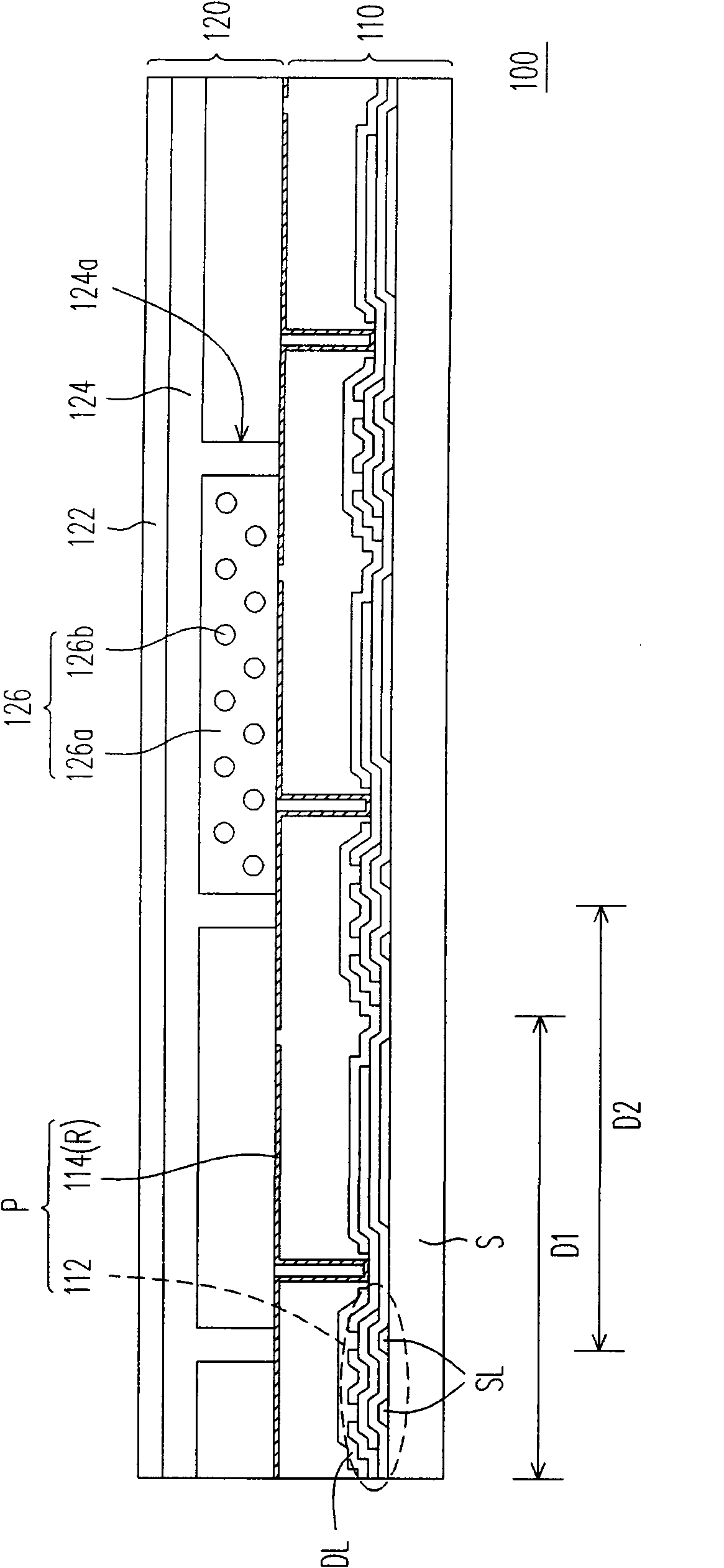
[0030] figure 1 It is a schematic cross-sectional view of the electrophoretic display panel according to the first embodiment of the present invention. Please refer to figure 1 The electrophoretic display panel 100 of this embodiment includes an active device array substrate 110 and an electrophoretic display film 120 . The active device array substrate 110 includes a plurality of active devices 112 and a light shielding layer 114 covering the active devices 112 . The electrophoretic display film 120 is disposed on the active device array substrate 110 , and the electrophoretic display film 120 includes a conductive layer 122 , a dielectric layer 124 and a plurality of electrophoretic display media 126 . Such as figure 1 As shown, the dielectric layer 124 is disposed on the lower surface of the conductive layer 122, the dielectric layer 124 has a plurality of microcups 124a arranged in an array and located on its lower surface, and the dielectric layer 124 is located betwee...
no. 2 example
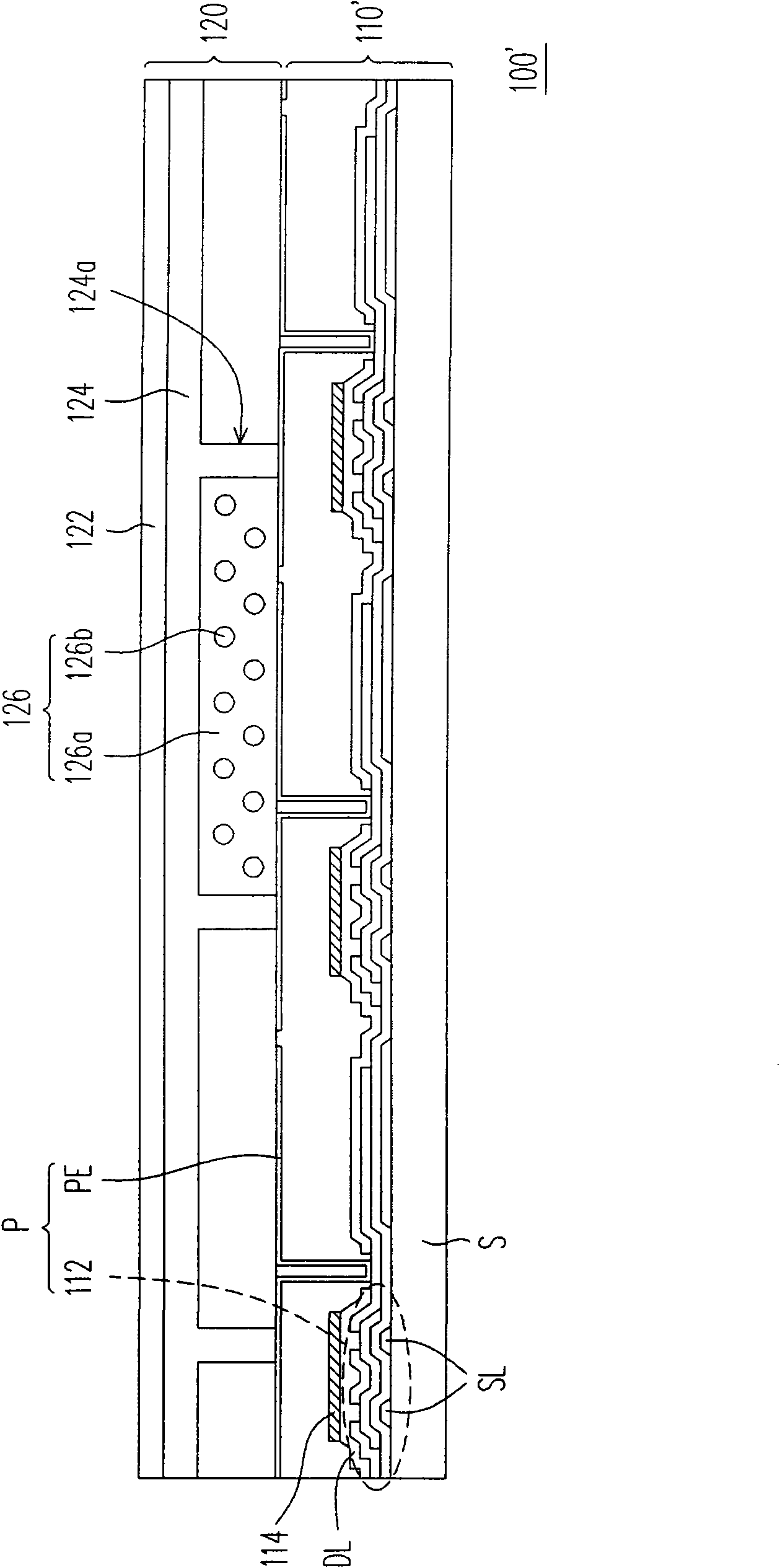
[0036] figure 2It is a schematic cross-sectional view of the electrophoretic display panel according to the second embodiment of the present invention. Please refer to figure 2 , the electrophoretic display panel 100' in this embodiment is similar to the electrophoretic display panel 100 in the first embodiment, but the main difference between them is that the light shielding layer 114 in the active element array substrate 110' in this embodiment is located Between the pixel electrode PE and the active device 112 , and the active device 112 and the pixel electrode PE form a plurality of pixels P. In other words, the light-shielding layer 114 and the pixel electrode PE belong to different film layers, which are different from the reflective pixel electrode R of the first embodiment.
[0037] Based on the above, the light-shielding layer 114 of this embodiment can be a metal layer with a single-layer structure, a metal layer with a multi-layer structure, a light-shielding la...
PUM
 Abstract
Description
Claims
Application Information

