Thin SOI longitudinal bipolar transistor and manufacturing method thereof

A technology of bipolar transistor and manufacturing method, applied in semiconductor/solid-state device manufacturing, semiconductor devices, electrical components, etc., can solve the complex process, large capacitance between base and emitter and collector, and quasi-precision requirements Advanced problems, to achieve the effect of reducing the difficulty of the process, improving the frequency performance, and reducing the complexity of the process

Active Publication Date: 2010-06-02
SHANGHAI HUAHONG GRACE SEMICON MFG CORP
View PDF0 Cites 3 Cited by
  • Summary
  • Abstract
  • Description
  • Claims
  • Application Information

AI Technical Summary

Problems solved by technology

[0008] like figure 1 The disadvantages of the prior art shown include the following points: 1. Two ion implantation processes are required to form the base connection region 41 and the base lead-out region 42 respectively, which makes the process complicated. In addition, the ion implantation of the base connection region 41 Alignment accuracy requirements are high, which further aggravates the process complexity; ②, the base current flows along the edge of the third isolation structure 22 through the silicon base region 40 and the base connection region 41 to the base lead-out region 42 and is drawn out therefrom, The resistance of the base path, that is, the base input resistance Rb is relatively large, thereby reducing the frequency performance of the current Ib and BJT; ③, the base connection region 41 is in contact with the collector region 30 and the silicon emitter region 50, and the collector region 30 is in contact with both the silicon base region 40 and the base connection region 41, resulting in large inter-electrode capacitances between the base, the emitter and the collector, which affects the frequency performance of the BJT

Method used


Image

  • Thin SOI longitudinal bipolar transistor and manufacturing method thereof
  • Thin SOI longitudinal bipolar transistor and manufacturing method thereof
  • Thin SOI longitudinal bipolar transistor and manufacturing method thereof

Examples


Embodiment Construction

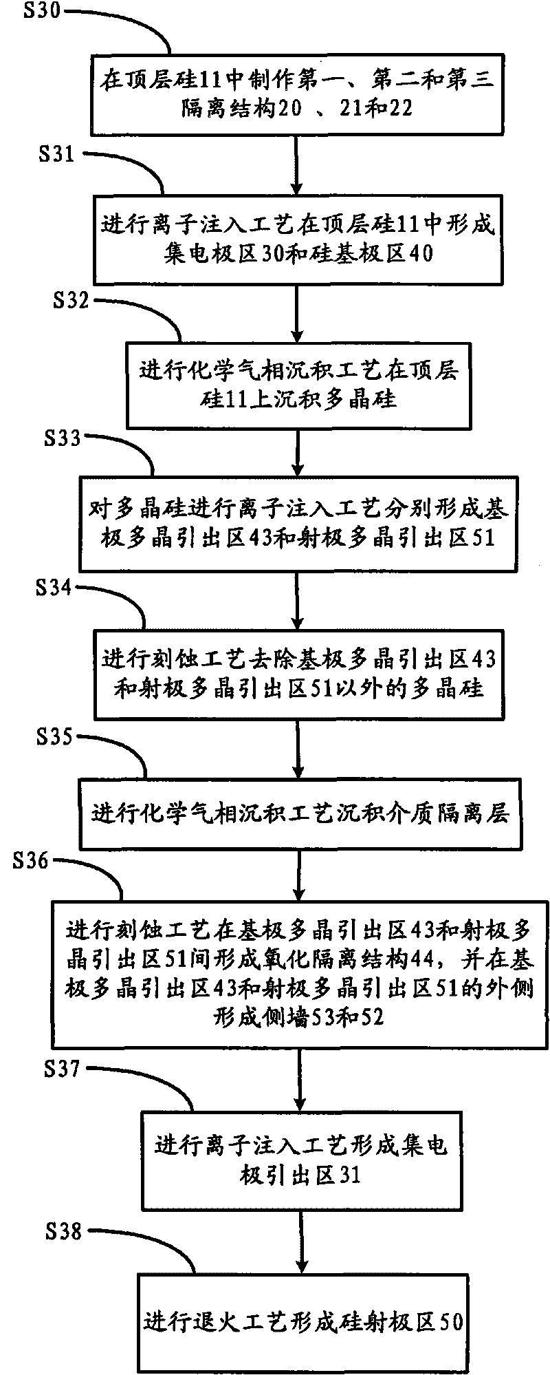
[0026] The thin SOI vertical bipolar transistor of the present invention and its manufacturing method will be further described in detail below.

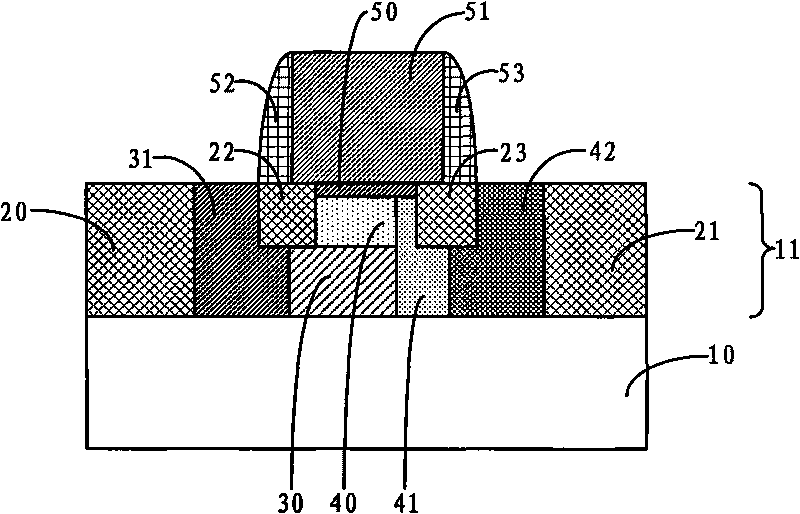
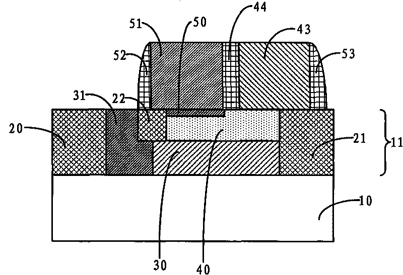
[0027] see figure 2 , which shows the composition structure of the thin SOI vertical bipolar transistor of the present invention, as shown in the figure, the thin SOI vertical bipolar transistor of the present invention is fabricated in the top layer silicon 11 and located in the first and second isolation structures 20 and 21, the top layer of silicon 11 is fabricated on the insulating buried layer 10, and there is also a third isolation structure 22 in the top layer of silicon 11. Under the insulating buried layer 10 is a silicon substrate (not shown), and the insulating buried layer 10 is usually silicon oxide. The thin SOI vertical bipolar transistor of the present invention includes a collector region 30, a silicon base region 40, a silicon emitter region 50, a collector lead-out region 31, a polycrystalline base region 43 and...


PUM


Abstract

The invention provides a thin SOI longitudinal bipolar transistor and a manufacturing method thereof. In the prior art, a base lead-out region is manufactured in top silicon and is connected with a silicon base region through a base connecting region, which causes the problems of complicated process, over-high base input resistance and interelectrode capacitance, and poor frequency performance ofthe transistor. The transistor of the invention, which is manufactured in the top silicon and is positioned between a first isolation structure and a second isolation structure, comprises a collectorregion, a silicon base region and a silicon emitter region which are sequentially stacked, wherein a collector lead-out region is arranged between the first isolation structure and a third isolation structure, is connected with the collector region, and is isolated from the silicon base region and the silicon emitter region through the third isolation structure; a polycrystalline base region and a polycrystalline emitter region are arranged on the top silicon in parallel; a medium isolation structure is arranged between the polycrystalline base region and the polycrystalline; the opposite outsides of the polycrystalline base region and the polycrystalline are provided with side walls; and the polycrystalline base region and the polycrystalline are connected with the silicon base region and the silicon emitter region respectively. The thin SOI longitudinal bipolar transistor and the manufacturing method thereof can reduce process complexity, effectively reduce the base input resistanceand the interelectrode capacitance, and effectively improve the frequency performance of the transistor.

Description

technical field [0001] The invention relates to the field of bipolar transistors, in particular to a thin SOI vertical bipolar transistor and a manufacturing method thereof. Background technique [0002] As the feature size of integrated circuits continues to decrease and enter the nanometer stage, the existing bulk silicon materials and processes are approaching their physical limits. To further improve the integration and operating speed of integrated circuits, it is necessary to improve materials and processes There are new major breakthroughs. Silicon on Insulator (Silicon On Insulator; SOI for short) is a major breakthrough in materials at present. It is recognized by the industry as one of the solutions to replace the existing monocrystalline silicon materials in the era of nanotechnology, and it is a major factor in maintaining the trend of Moore's Law. weapon. [0003] SOI has a three-layer structure of "top silicon-insulating buried layer-silicon substrate", which...

Claims


Application Information

Patent Timeline
Patent Type & Authority Applications(China)
IPC IPC(8): H01L29/732H01L21/331
Inventor 周建华陈天兵彭树根高明辉
Owner SHANGHAI HUAHONG GRACE SEMICON MFG CORP
Why Eureka
Try Eureka