Wafer tester and testing method thereof

A wafer testing and wafer technology, which is applied in the wafer testing apparatus and its testing field, can solve the problems of microcircuit damage, inability to provide the amount of pressure under the probe card, and probe failure damage.

Inactive Publication Date: 2010-06-16
KING YUAN ELECTRONICS
View PDF1 Cites 20 Cited by
  • Summary
  • Abstract
  • Description
  • Claims
  • Application Information

AI Technical Summary

Problems solved by technology

[0004] However, the above-mentioned prior art can only know the contact status of the probes and the wafer in a passive manner. If it is known that there is a poor contact between the probes and the wafer, it is still necessary to manually press down the probe card to deal with the lack of contact. A good probe cannot provide an automated way to directly adjust the downforce of the probe card, so it still affects the test yield and efficiency of the wafer in actual use
In addition, if the speed or force of the wafer testing device platform approaching the probe card is abnormal or unstable, even probes with elastic contact structures or buffer material components have limited buffer force, which may still cause damage to the microcircuits on the wafer surface. damage, and even cause probe failure to damage the

Method used


Image

  • Wafer tester and testing method thereof
  • Wafer tester and testing method thereof
  • Wafer tester and testing method thereof

Examples


Embodiment Construction

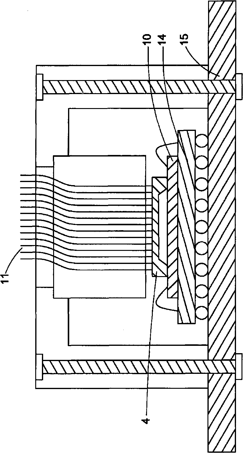
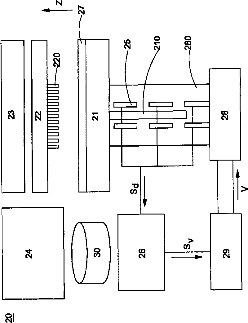
[0018] Please refer to figure 2 , is the first preferred embodiment proposed by the present invention, and is a schematic diagram of a wafer testing device. This wafer testing device 20 includes a wafer carrying platform 21, a probe card 22, a test carrier board 23, a test bench 24, a plurality of converters 25, and a feedback device 26, wherein the wafer carrying platform 21 is used To carry a wafer 27 to be tested, and this wafer carrying platform 21 is connected with a base 28 by a transmission mechanism 280, and the base is further connected with a driving motor 29, thus driving the motor 29 to provide wafer carrying The movement of the platform 21 in the X-Y-Z three-axis direction. The probe card 22 includes a plurality of probes 220 for detecting the wafer 27 to be tested on the wafer carrying platform 21 . The test carrier board 23 is a printed circuit board, one end of which is connected to the probe card 22 and the other end is connected to the test bench 24, and s...


PUM


Abstract

The invention provides a wafer tester and a testing method thereof. The wafer tester comprises a wafer bearing platform, a probe card, a plurality of converters, a testing carrier plate, a test board and a feedback device, wherein the wafer bearing platform provides movement of three axes of X, Y and Z so as to bear a wafer to be tested; the probe card comprises a plurality of probes for testing the wafer to be tested of the wafer bearing platform; the plurality of the converters are arranged on a Z-axis path of the wafer bearing platform moving towards the probe card respectively; when each converter detects that the wafer bearing platform displaces along the Z axis, a displacement electronic signal is output to the feedback device; the feedback device receives the displacement electronic signal so as to adjust a moving speed of the wafer bearing platform along the Z axis and further make the wafer on the wafer bearing platform contact the probes of the probe card in a micro-contact mode, which can avoid that the probes of the probe card directly damage a micro-circuit of the wafer caused by an inappropriate Z-axis speed.

Description

technical field [0001] The present invention relates to a wafer test device and its test method, in particular to a wafer test device with a converter and a feedback device and its test method. Background technique [0002] When testing wafers of known technology, in order to avoid improper contact between the probes on the probe card and the wafer, thereby reducing the service life of the probe card and the wafer test yield, a sensor is usually added between the two. It can not only know whether the probes on the probe card are faulty or damaged, so as to improve the use efficiency of the probes and avoid damage to the microcircuits on the wafer, but also reduce the cost of the probes and the microcircuits on the wafer. The test yield of the wafer is reduced due to poor contact. [0003] Please refer to figure 1 , the prior art Taiwan China Patent TW569017 has disclosed a vertical probe card with force feedback, this probe card includes a thin film substrate 10, an array ...

Claims


Application Information

Patent Timeline
Patent Type & Authority Applications(China)
IPC IPC(8): G01R31/26G01R1/073
Inventor 张久芳
Owner KING YUAN ELECTRONICS
Why Eureka
Try Eureka