Touch panel

A touch panel and touch unit technology, which is applied in the fields of instruments, electrical digital data processing, and data processing input/output processes, etc., can solve the problem of misjudgment of the touch position of the touch panel.

Active Publication Date: 2014-07-23
INNOLUX CORP
View PDF4 Cites 0 Cited by
  • Summary
  • Abstract
  • Description
  • Claims
  • Application Information

AI Technical Summary

Problems solved by technology

[0008] However, when the user applies an external force to the touch panel 1, since the common electrode 15 is a one-piece structure, the local recessed area may include other non-touch positions in addition to the touch position.
At this time, it may cause misjudgment of the touch position by the touch panel 1

Method used


Image

  • Touch panel
  • Touch panel
  • Touch panel

Examples


no. 1 example

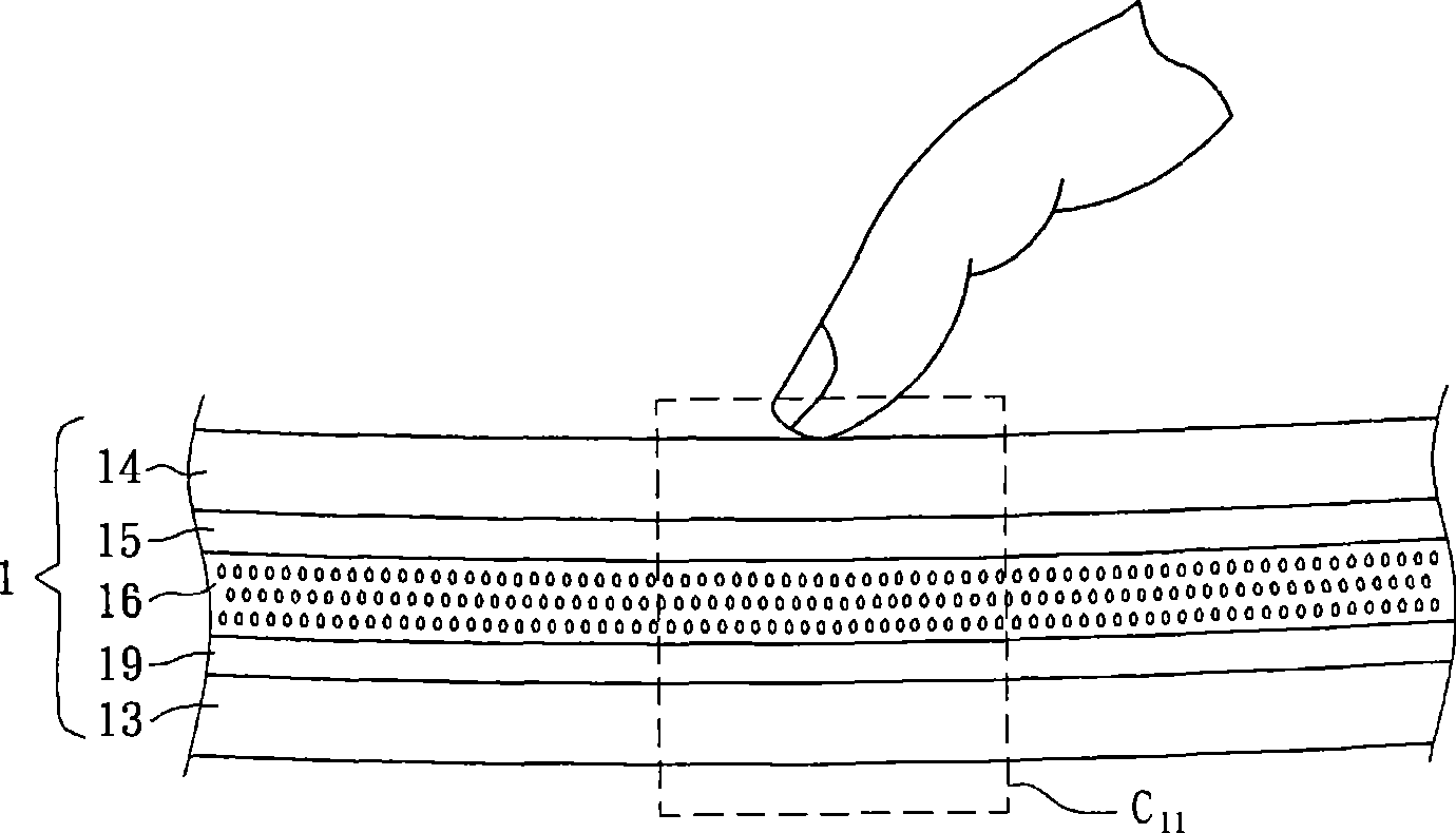
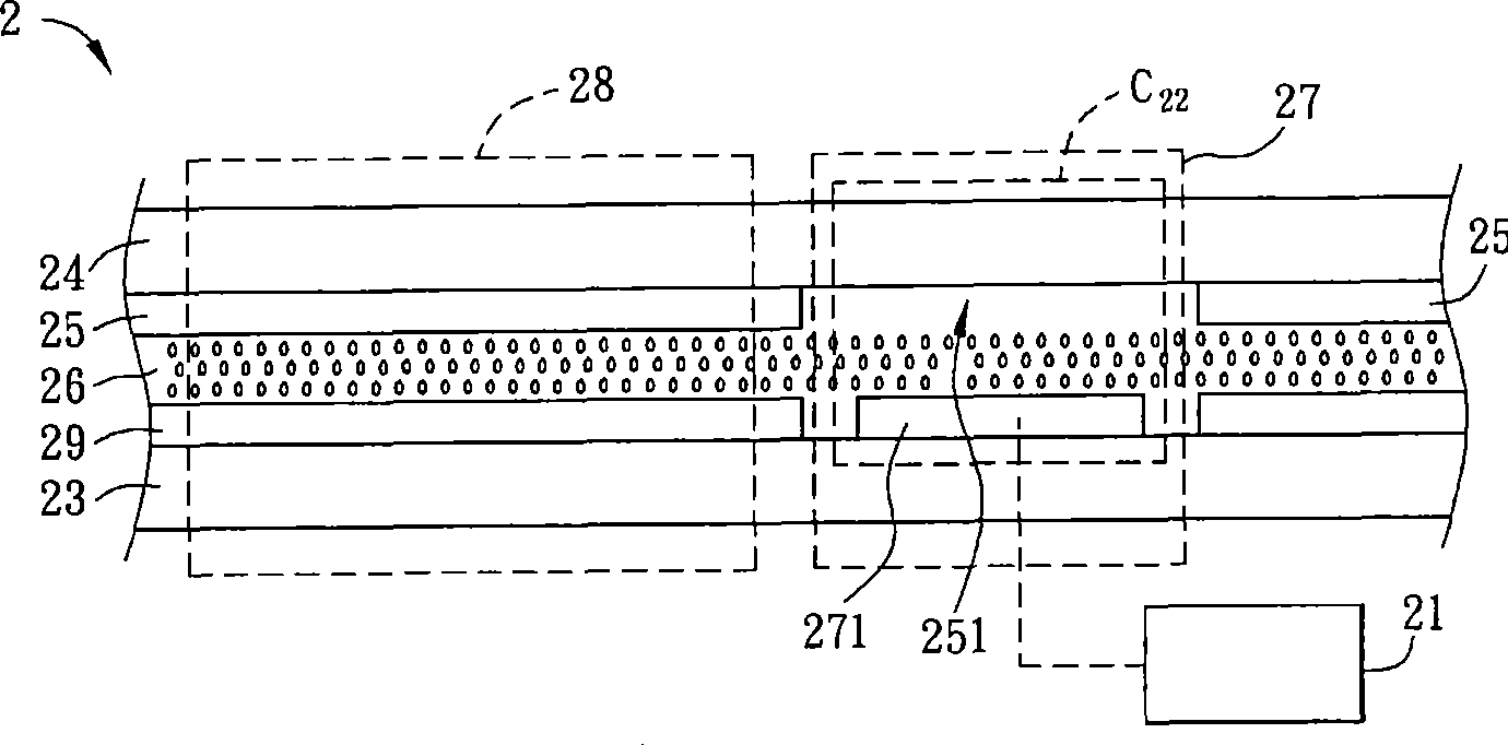
[0057] refer to figure 2 and image 3 As shown, among them, figure 2 It is a top view of the touch panel 2 according to the first embodiment of the present invention, image 3 for figure 2 Sectional view of line A-A in middle. The touch panel 2 according to the first embodiment of the present invention includes a thin film transistor substrate 23 , a color filter substrate 24 , a common electrode 25 and a liquid crystal layer 26 .

[0058] The TFT substrate 23 is disposed opposite to the color filter substrate 24 , and the liquid crystal layer 26 is disposed between the TFT substrate 23 and the color filter substrate 24 . In this embodiment, the TFT substrate 23 and the color filter substrate 24 can be glass substrates or plastic substrates respectively. The common electrode 25 is disposed on a side of the color filter substrate 24 close to the TFT substrate 23 , and the common electrode 25 has at least one opening 251 .

[0059] Continue to refer to image 3 As show...

no. 2 example

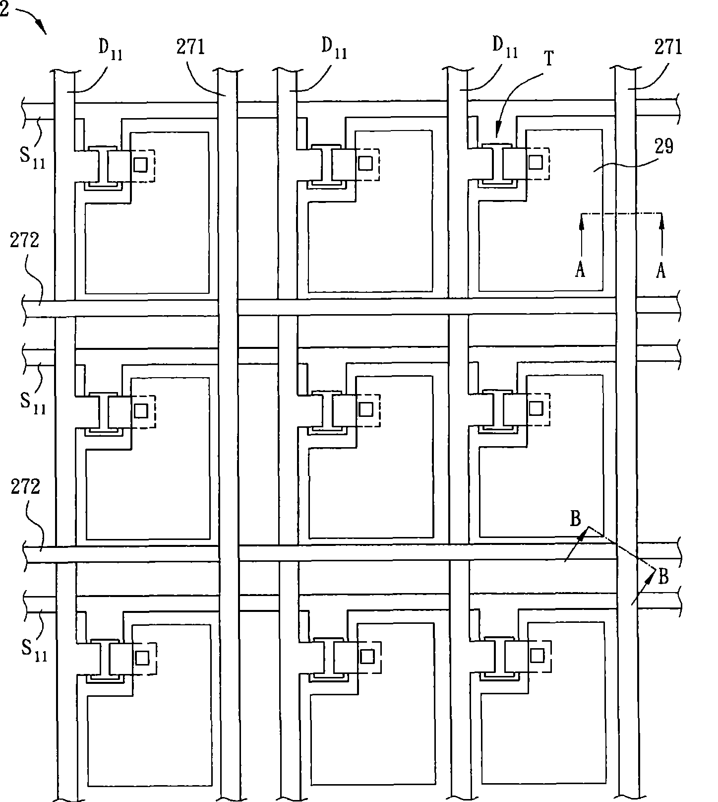
[0075] The sensing lines of the touch panel 2 can be designed not only on the side of the TFT substrate (as in the first embodiment), but also on the side of the color filter substrate. refer to Figure 6 As shown, the touch panel 3 of this embodiment includes a thin film transistor substrate 33 , a color filter substrate 34 , a common electrode 35 , a liquid crystal layer 36 , and a pixel unit 38 , wherein the pixel unit 38 includes a pixel electrode 39 .

[0076] in, Figure 6 In the thin film transistor substrate 33, the color filter substrate 34, the common electrode 35, the liquid crystal layer 36, the pixel unit 38 and the pixel electrode 39 and image 3 The thin film transistor substrate 23 , color filter substrate 24 , common electrode 25 , liquid crystal layer 26 , pixel unit 28 and pixel electrode 29 have the same connections and functions, which will not be repeated here.

[0077] Moreover, in this embodiment, the common electrode 35 may have an opening, or the co...

no. 3 example

[0085] Also refer to Figure 8A and Figure 8B as shown, Figure 8A is a top view of the touch panel 4 of the third embodiment, Figure 8B for Figure 8A Sectional view of line C-C in middle. The touch panel 4 of this embodiment includes a thin film transistor substrate 43 , a color filter substrate 44 , a common electrode 45 , a liquid crystal layer 46 , a pixel unit 48 and a pixel electrode 49 .

[0086] in, Figure 8B In the thin film transistor substrate 43, the color filter substrate 44, the common electrode 45, the liquid crystal layer 46, the pixel unit 48 and the pixel electrode 49 and image 3 The thin film transistor substrate 23 , color filter substrate 24 , common electrode 25 , liquid crystal layer 26 , pixel unit 28 and pixel electrode 29 have the same connections and functions, which will not be repeated here.

[0087] The touch unit 47 includes a sensing capacitor C 42 It also has a plurality of first sensing lines 471 and a plurality of sensing extensio...


PUM


Abstract

The invention discloses a touch panel which is provided a thin film transistor substrate and a color filter substrate, wherein the thin film transistor substrate is arranged opposite to the color filter substrate. A public electrode is arranged at one side of the color filter substrate near the thin film transistor substrate and is provided with a plurality of opening parts. The touch panel comprises an induction reading loop, a touch unit and at least one pixel unit, wherein the pixel unit is arranged near the touch unit; the touch unit is provided with a plurality of parallel first induction lines and is arranged at one side of the thin film transistor substrate near the color filter substrate, wherein each first induction line is arranged opposite to each corresponding opening part; and the pixel unit is provided with a pixel electrode and is arranged on the thin film transistor substrate, and the electric property of the pixel electrode is electrically controlled by a scan line and a data line.

Description

technical field [0001] The invention relates to a touch panel. Background technique [0002] With the continuous advancement of science and technology, various information devices are constantly being introduced. Wherein, as far as the data input device is concerned, in addition to generally inputting data with a keyboard or a mouse, using touch technology to input data is also another option for inputting data. In addition to vision and hearing, people also have a sense of touch, and with the continuous update and breakthrough of sensor technology, touch sensors have become another choice for people to communicate with information equipment. [0003] On the other hand, traditional computer input interfaces (such as keyboards or mice) have a certain degree of difficulty in operation for people who are not familiar with computers, and have become one of the obstacles to the popularization of computers. In order to provide a more intuitive operating device, recently, the ind...

Claims


Application Information

Patent Timeline
Patent Type & Authority Patents(China)
IPC IPC(8): G02F1/133G06F3/041
Inventor 李国胜朱正仁
Owner INNOLUX CORP
Why Eureka
Try Eureka