Structure and method thereof for testing reliability of gate oxide of high-voltage MOS device

A technology of MOS devices and gate oxide layers, applied in semiconductor/solid-state device testing/measurement, electric solid-state devices, semiconductor devices, etc., can solve problems such as fusing and hindering the continuous progress of reliability testing, so as to ensure connection and improve efficiency Effect

Active Publication Date: 2010-06-23
HEJIAN TECH SUZHOU
View PDF0 Cites 8 Cited by
  • Summary
  • Abstract
  • Description
  • Claims
  • Application Information

AI Technical Summary

Problems solved by technology

Therefore, in some cases, when the gate oxide layer of the component under test is not broken down, it is fused due to the high power carried by the metal connection, which hinders the sustainable performance of the reliability test.

Method used


Image

  • Structure and method thereof for testing reliability of gate oxide of high-voltage MOS device
  • Structure and method thereof for testing reliability of gate oxide of high-voltage MOS device
  • Structure and method thereof for testing reliability of gate oxide of high-voltage MOS device

Examples


Embodiment Construction

[0012] In order to make the above-mentioned purposes, features and advantages of the present invention more obvious and easy to understand, the accompanying drawings of the embodiment of the reliability test structure are described in detail as follows:

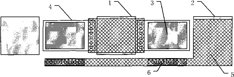
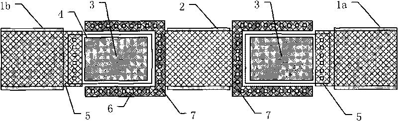
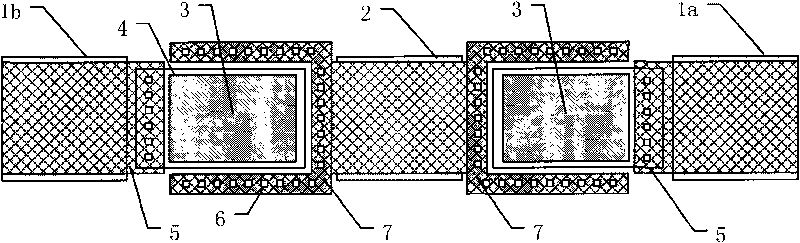
[0013] Such as figure 2 As shown, the present invention provides a test structure for the reliability of the gate oxide layer of a high-voltage MOS device, including a gate 1a, a gate 1b, a base 2, a diffusion layer 3, a polycrystalline 4, a metal layer 5 and a ring of a high-voltage MOS device. Shaped protective structure 7. The annular protection structure 7 is composed of a stacked diffusion layer 3, a metal layer 5 and an interlayer via hole 6, and the gate 1a and the gate 1b are independent contact pads, which are respectively arranged on both sides of the common base 2; at the same time , the ring-shaped protective structure 7 is surrounded by the test structure in a partially surrounded manner.

[0014] In addition,...


PUM


Abstract

The invention relates to a structure and a method thereof for testing reliability of a gate oxide of a high-voltage MOS device. Different current-voltage source probes for testing are respectively connected with a gate electrode and a base electrode. To increase the area of the gate oxide for testing in a single testing key, a structure with a plurality of same repeated structures (usually 2) connected in parallel is adopted, wherein the gate electrode of each repeated structure uses a relatively independent contact pad, shares the grounded base electrode, and surrounds the testing structure by an annular protection structure part; the gate electrode contact pads at two sides are connected with different current-voltage source probes; and each current-voltage source synchronously outputs testing voltage and measures the corresponding current. The design scheme of the invention ensures execution stability of reliability test and also improves efficiency of the reliability test.

Description

technical field [0001] The invention relates to semiconductor devices, in particular to a testing process structure for the reliability of gate oxide layers of high-voltage MOS devices, and belongs to the field of semiconductor manufacturing. Background technique [0002] With the miniaturization of semiconductor integrated chips, in the reliability test of the gate oxide layer of high-voltage MOS devices, since the line width of the feature size is getting smaller and smaller, the size of the reliability test key will be correspondingly smaller. The line width of the line will also be narrowed accordingly. When some test structures need to accumulate a certain area or a certain length, it is often necessary to repeat the same structure several times (at least 2), so that the metal connections of some common terminals will inevitably be elongated. Such as figure 1 The existing test structure shown is: a common gate terminal 1 and a common base terminal 2 are used, several ...

Claims


Application Information

Patent Timeline
IPC IPC(8): H01L23/544H01L21/66
Inventor 张瑜劼彭昶
Owner HEJIAN TECH SUZHOU
Why Eureka
Try Eureka