Electrostatic protection structure and manufacturing method thereof

A protection structure, anti-static technology, applied in the direction of circuits, electrical components, electrical solid devices, etc., can solve the problems of low resistance of the horizontal triode path, physical damage of the field oxidation area, etc., to avoid physical damage and improve stability.

Active Publication Date: 2010-06-23
SHANGHAI HUAHONG GRACE SEMICON MFG CORP
View PDF0 Cites 12 Cited by
  • Summary
  • Abstract
  • Description
  • Claims
  • Application Information

AI Technical Summary

Problems solved by technology

However, it is found in the research that a large electric field is easily generated at the intersection of the N+ diffusion region of the drain and the field oxide region near the gate side, such as figure 1 As shown by the middle arrow, the concentration of N-type impurities in the drain region is higher on the surface than in the deep layer of silicon, so that the path resistance of the horizontal triode is smaller than that of the vertical triode, and more ESD current passes through the conduction path of the horizontal triode. , a large current will also pass through this junction, generating a lot of heat. When the temperature is too high, it will cause physical damage to the field oxidation zone here

Method used


Image

  • Electrostatic protection structure and manufacturing method thereof
  • Electrostatic protection structure and manufacturing method thereof
  • Electrostatic protection structure and manufacturing method thereof

Examples


Embodiment Construction

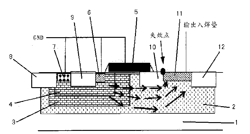
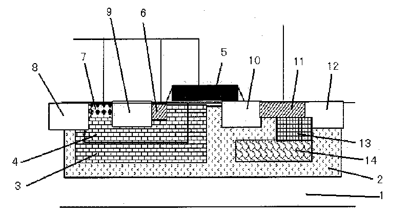
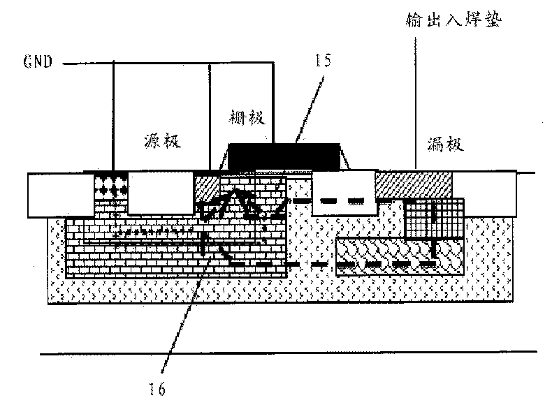
[0017] The invention discloses an antistatic protection structure, such as image 3 As shown, it includes a P-type substrate 1 and an N-type deep well 2 on it, and a P well is arranged on the N-type deep well 2, and the P well includes a high-voltage P well 3 and a high-voltage P well 3 contained in the high-voltage P well 3. A low-voltage P well 4, the P well and the N-type deep well 2 are provided with a first polysilicon gate 5, the left part of the first polysilicon gate 5 covers the high-voltage P well 3 and the low-voltage P well 4, and the right partly covers the N-type deep well 2, a first N+ diffusion region 6 is arranged on the lower left side of the first polysilicon gate 5, and a P+ diffusion region 7 is also arranged on the left side of the first N+ diffusion region 6, so A first field oxidation region 8 is provided on the left side of the P+ diffusion region 7, a second field oxidation region 9 is separated between the P+ diffusion region 7 and the first N+ diffu...


PUM


Abstract

The invention discloses an electrostatic protection structure, which comprises a P-type substrate and an N-type deep well on the P-type substrate, wherein an N well is further arranged below a second N+ diffusion region and a fourth field oxide region and in the range of the N-type deep well; and an N-type secondary diffusion region is further arranged below the N well. The invention further discloses a manufacturing method for the electrostatic protection structure, wherein the N-type secondary diffusion region is formed by an ion implantation process after the formation of the field oxide region and before the formation of the N well. The electrostatic protection structure and the manufacturing method can ensure uniform distribution of current during current discharge by arranging the N-type secondary diffusion region under the N-type well, so physical damage caused to the electrostatic protection structure is avoided and the stability of the device is improved.

Description

technical field [0001] The invention relates to an antistatic protection structure of a semiconductor device, and also relates to a manufacturing method of the antistatic protection structure of a semiconductor device. Background technique [0002] The damage of static electricity to electronic products has always been a problem that is not easy to solve. The most commonly used ESD protection structure today uses the GGNMOS structure (Ground Gate NMOS, gate grounded NMOS), but it is mainly used in the electrostatic protection of low-voltage circuits. At present, the more popular electrostatic protection structure applied to high-voltage circuits is lateral diffusion NMOS (Lateral Diffusion NMOS), such as figure 1 As shown, it includes a P-type substrate 1 and an N-type deep well 2 on it, and a P well is arranged on the N-type deep well 2, and the P well includes a high-voltage P well 3 and a high-voltage P well 3 contained in the high-voltage P well 3. A low-voltage P well ...

Claims


Application Information

Patent Timeline
Patent Type & Authority Applications(China)
IPC IPC(8): H01L23/60H01L21/00
Inventor 苏庆吕赵鸿
Owner SHANGHAI HUAHONG GRACE SEMICON MFG CORP
Why Eureka
Try Eureka