Cantilever beam type accelerometer based on photonic crystal microcavity

A photonic crystal microcavity and cantilever beam technology, which is applied in the direction of measurement of acceleration, velocity/acceleration/shock measurement, optical waveguide coupling, etc., can solve the problems of difficult improvement of performance parameters such as resolution and sensitivity, and expand the scope of application , light weight and wide application range

Inactive Publication Date: 2010-07-21
ZHONGBEI UNIV
View PDF1 Cites 12 Cited by
  • Summary
  • Abstract
  • Description
  • Claims
  • Application Information

AI Technical Summary

Benefits of technology

This new type of sensor called an optronic chip (OCh) allows for precise measurements over extreme environmental factors like pressure, temperature, humidity levels, etc., without being affected by external influences from other things around them. Its technical effect includes improved performance due to increased flexure properties compared to previous designs while maintaining good signal quality at low temperatures.

Problems solved by technology

This patented technical problem addressed in this patents relates to improving the accuracy and resolvability of miniature electronic devices made using MEMS techniques due to their ability to generate minute forces caused by external stimuli without being affected by gravity effects during operation. These tiny movements cause errors when measuring physical quantities. To address this issue, there was proposed a new type of sensor called Planck Microcanostor Accelerometry (PCA). PCA allows for precise measurements while maintaining stability against gravitational impact.

Method used


Image

  • Cantilever beam type accelerometer based on photonic crystal microcavity
  • Cantilever beam type accelerometer based on photonic crystal microcavity
  • Cantilever beam type accelerometer based on photonic crystal microcavity

Examples


Embodiment Construction

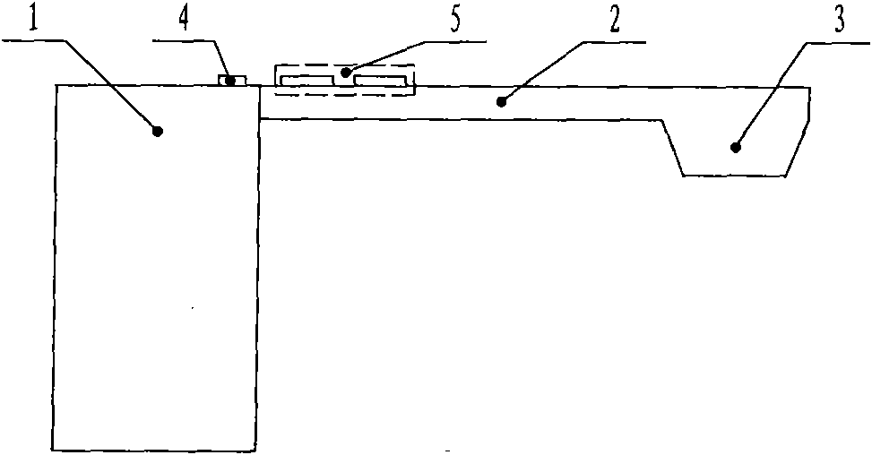
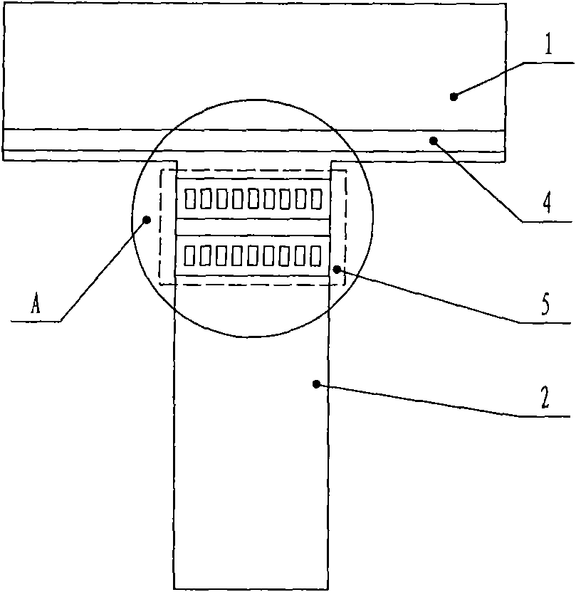
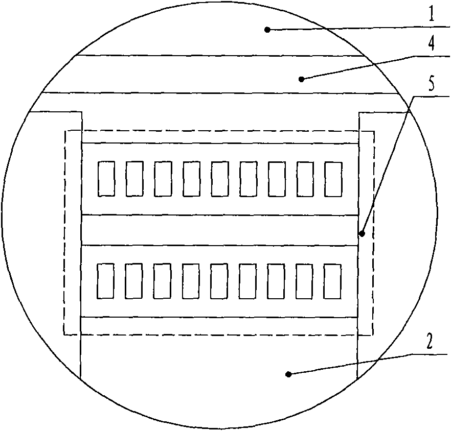
[0017] like Figure 1-3 As shown, the cantilever beam accelerometer based on the photonic crystal microcavity includes the base 1 processed on the semiconductor substrate by the micro-electromechanical device processing technology (MEMS processing technology), and the cantilever beam fixed to the base 1 at one end 2. The mass block 3 fixed to the free end of the cantilever beam 2, the base 1 is provided with an optical waveguide 4 perpendicular to the cantilever beam 2, and the end of the cantilever beam 2 fixed to the base 1 is provided with a "zipper cavity (Zippercarity) 5. The two brackets of the "zipper cavity" 5 are parallel to the optical waveguide 4 on the base 1, and the "zipper cavity" 5 and the optical waveguide 4 form a microcavity-optical waveguide coupling structure.

[0018] During specific implementation, the material of the "zipper hole" 5 is silicon nitride Si 3 N 4 , the material of the optical waveguide is silicon dioxide SiO 2 In the cantilever beam str...


PUM


Abstract

The invention relates to an optical and microelectromechanical technology, in particular to a cantilever beam type accelerometer based on a photonic crystal microcavity. The application of the photonic microcavity in the cantilever beam type accelerometer is further expanded. The cantilever beam type accelerometer based on the photonic crystal microcavity comprises a base, a cantilever beam and a mass block, wherein the base is processed on a semiconductor substrate by a processing process of a microelectromechanical device; the single end of the cantilever beam is fixed to the base; the mass block is fixed to the free end of the cantilever beam; an optical waveguide which is perpendicular to the cantilever beam is arranged on the base; the end part of the cantilever beam, which is fixed to the base, is provided with a zipper cavity; two brackets of the zipper cavity are parallel to the optical waveguide on the base; and the zipper cavity and the optical waveguide form a microcavity-optical waveguide coupling structure. The invention has reasonable and simple structure and good characteristics of high sensitivity, high resolution, high measurement precision, electromagnetic interference resistance, small size, convenient integration, light weight, operation in severe environment, wide application range, and the like.

Description


Claims


Application Information

Patent Timeline
Owner ZHONGBEI UNIV
Why Eureka
Try Eureka