Ion implantation method of semiconductor component

An ion implantation and component technology, which is applied in semiconductor/solid-state device manufacturing, electrical components, circuits, etc., and can solve problems such as short circuits, failure of semiconductor components, and inability to conduct effective control.

Active Publication Date: 2012-05-30
SEMICON MFG INT (SHANGHAI) CORP
View PDF0 Cites 0 Cited by
  • Summary
  • Abstract
  • Description
  • Claims
  • Application Information

AI Technical Summary

Problems solved by technology

When ion implantation is performed, the implanted ions enter a deep position in the above-mentioned polysilicon layer due to the above-mentioned channel effect, and even penetrate the gate under the polysilicon layer, and a punch-through phenomenon occurs, so that the Source (Source) ) and the channel between the drain (Drain) is short-circuited, so that the gate cannot effectively control the conduction of the channel between the source and the drain, resulting in the failure of semiconductor components

Method used


Image

  • Ion implantation method of semiconductor component
  • Ion implantation method of semiconductor component
  • Ion implantation method of semiconductor component

Examples


Embodiment Construction

[0019] In order to make the object, technical solution and advantages of the present invention more clearly, the present invention will be further described in detail below in conjunction with the accompanying drawings and specific embodiments.

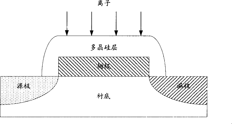
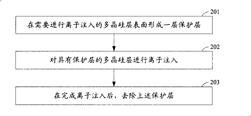
[0020] figure 2 It is a schematic flow chart of the ion implantation method for semiconductor components in the present invention. Such as figure 2 As shown, the ion implantation method of semiconductor components provided in the present invention includes the following steps:

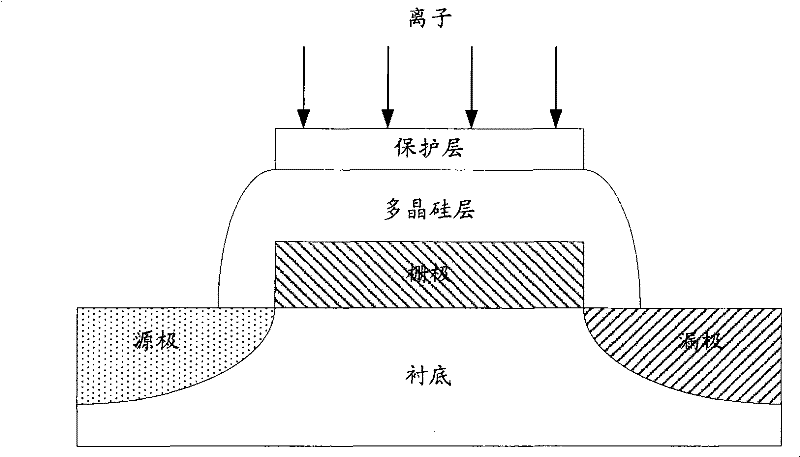
[0021] In step 201, a protective layer (Prevent Layer) is formed on the surface of the polysilicon layer to be ion-implanted.

[0022] image 3 It is a schematic diagram of the ion implantation method of semiconductor components in the present invention. Such as image 3 As shown, in this step, a protective layer can be formed on the surface of the polysilicon layer to be ion-implanted by a deposition method or a growth method commonly used in the prior...


PUM


Abstract

The invention discloses an ion implantation method of a semiconductor component. The ion implantation method comprises the following steps of: forming a protection layer on the surface of a polysilicon layer that needs to carry out ion implantation; carrying out the ion implantation on the polysilicon layer with the protection layer; and removing the protection layer after the ion implantation isfinished. By using the ion implantation method, the implanted ions are distributed in the polysilicon layer more evenly, and the punching through phenomenon is avoided, therefore, the better doping effect can be obtained, and the performance of the semiconductor component is improved.

Description

technical field [0001] The invention relates to the manufacturing technology of semiconductor components, in particular to an ion implantation method of semiconductor components. Background technique [0002] In the manufacturing technology of semiconductor components, since the conductivity of silicon in a pure state is very poor, only when a small amount of impurities are added to silicon to change the structure and conductivity of silicon, silicon can become a useful semiconductor. , The above-mentioned process of adding a small amount of impurities to silicon is called doping. Silicon doping technology is the basis for preparing semiconductor components, and ion implantation (Ion Implant) technology is one of the most important doping methods. Since ion implantation technology can repeatedly control the concentration and depth of doped impurities, it has become a standard process to meet the requirements of sub-0.25 micron feature size and large-diameter silicon wafer p...

Claims


Application Information

Patent Timeline
Patent Type & Authority Patents(China)
IPC IPC(8): H01L21/265H01L21/31
Inventor 何有丰唐兆云
Owner SEMICON MFG INT (SHANGHAI) CORP
Why Eureka
Try Eureka