Check patentability & draft patents in minutes with Patsnap Eureka AI!

Method for making packaging substrate with recess structure

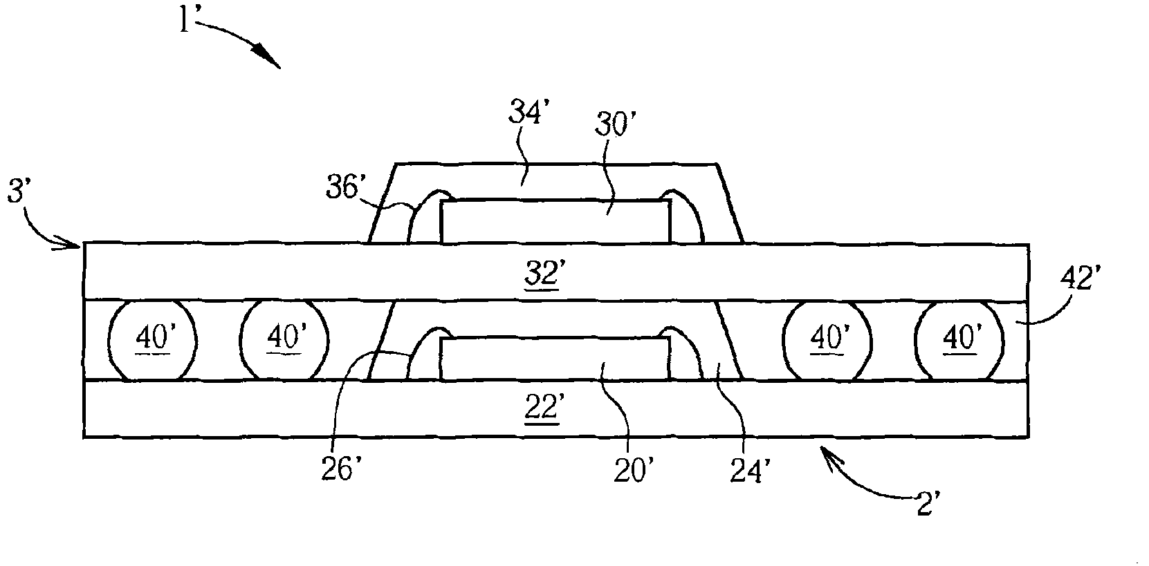
A technology for packaging substrates and manufacturing methods, which is applied in the manufacture of semiconductor/solid-state devices, assembling printed circuits with electrical components, and electrical components, etc., can solve the problem of small packaging process margins, the difficulty of increasing the number of output and input pins of 40' of solder balls, Problems such as the first substrate 22' and the second substrate 32' are additionally performed

Active Publication Date: 2010-07-28
UNIMICRON TECH CORP
View PDF0 Cites 19 Cited by
  • Summary
  • Abstract
  • Description
  • Claims
  • Application Information

AI Technical Summary

Problems solved by technology

[0004] The above-mentioned conventional package-on-package structure includes at least the following disadvantages: (1) The size of the solder ball 40' is limited by the distance between the first substrate 22' and the second substrate 32'
The height of the solder balls 40' must exceed the height of the molding material 24' to ensure the electrical connection between the first substrate 22' and the second substrate 32', so the pitch of the solder balls cannot be further reduced, resulting in solder balls The number of balls 40' and the number of input / output pins (I / O) are difficult to increase; (2) the coefficient of thermal expansion (CTE) of the first substrate 22' and the second substrate 32' is different, so that the solder balls 40' may be affected to different degrees. Stress affects the reliability of the package; (3) it is not easy to control the coplanarity of the solder ball 40', so that the margin (process window) of the packaging process is small; (4) the first substrate 22' and the second substrate need to be additionally The glue filling step between the two substrates 32'; (5) the stacking volume is relatively large

Method used


Image

  • Method for making packaging substrate with recess structure
  • Method for making packaging substrate with recess structure
  • Method for making packaging substrate with recess structure

Examples


Embodiment Construction

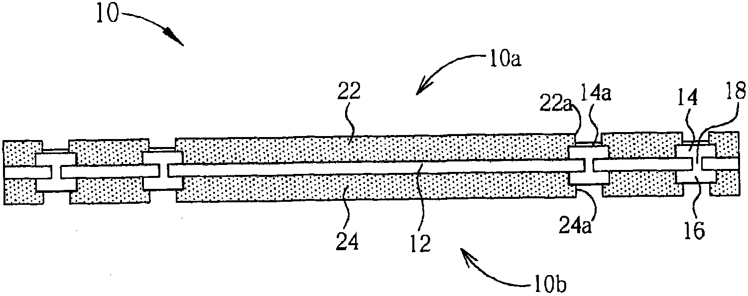
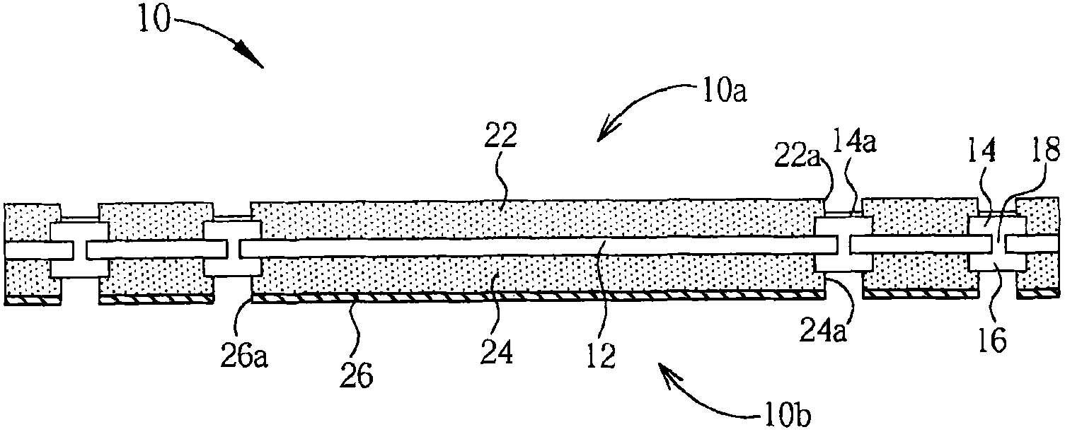
[0045] The invention relates to a manufacturing method of a packaging substrate with a cavity structure, which is used as a solution for integrating high-density integrated circuit components. The invention utilizes a pressing process of a composite circuit board to combine the circuit board with reserved openings with the main body circuit board to complete the packaging substrate with a cavity structure.

[0046] The manufacturing method of the packaging substrate with cavity structure of the present invention can be mainly divided into three parts, wherein the first part is to form the connection board with reserved openings, the second part is to form the main circuit board, and the third part is to form the connection board Press fit with the main circuit board. Below, that is, through Figure 1a to Figure 1c Explain the first part, by Figure 2a and Figure 2b Explain the second part, by image 3 Describe the third part.

[0047]see Figure 1a to Figure 1c , which ...


PUM


Abstract

The invention discloses a method for making a packaging substrate with a recess structure. The method comprises the following steps of: providing a connecting plate which comprises a first circuit layer, a first solder mask layer covered on the first circuit layer and a joint layer arranged on the first solder mask layer; providing a main body circuit board which at least comprises a second circuit layer and a second solder mask layer covering the second circuit layer, wherein the second solder mask layer comprises a plurality of openings for exposing part of the second circuit layer; forming a plurality of conductive bump structures in the plurality of openings; and laminating the connecting plate and the main body circuit board to ensure that the conductive bump structures are firmly coated and laminated in a structure consisting of the first solder mask layer, the joint layer and the second solder mask layer.

Description

technical field [0001] The invention relates to a method for manufacturing a packaging substrate, in particular to a method for manufacturing a high-density packaging substrate with a cavity structure. Background technique [0002] In recent years, the rapid development of three-dimensional (3D) packaging has not only greatly reduced the area occupied by the memory on the circuit board, but also improved the efficiency of electronic products after shrinking, and can integrate chips with different functions into the same packaging module. , to achieve high benefits of System in Package (SiP). Among them, the package-on-package structure (PoP) is a type of three-dimensional structure. For example, the package-on-package structure can greatly reduce high-level components by integrating high-capacity memories and complex processors. The circuit board space of the mobile phone. [0003] figure 1 What is shown is a schematic cross-sectional structure diagram of a traditional pa...

Claims


Application Information

Patent Timeline
IPC IPC(8): H01L21/603H01L23/492H01L23/12H05K3/32
CPCH01L2224/48228H01L2224/48091H01L2224/48227
Inventor 陈国庆陈宗源
Owner UNIMICRON TECH CORP
Features
  • R&D
  • Intellectual Property
  • Life Sciences
  • Materials
  • Tech Scout
  • Unparalleled Data Quality
  • Higher Quality Content
  • 60% Fewer Hallucinations
Learn More