

Processing technology of protective plate of PCB (Printed Circuit Board) testing device
A technology of processing technology and testing device, which is applied in the field of PCB testing device guard plate processing technology, can solve the problems of test device failure, large gap between the pinhole of the guard plate and the needle bar of the test needle, loss of elasticity, etc.
Inactive Publication Date: 2010-08-04
TPV ELECTRONICS (FUJIAN) CO LTD
View PDF5 Cites 6 Cited by
- Summary
- Abstract
- Description
- Claims
- Application Information
AI Technical Summary
Problems solved by technology
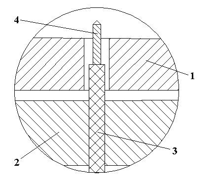
[0002] In the current PCB testing device, such as figure 1 As shown, there is a large gap between the pinhole of the guard plate and the needle bar of the test needle, which cannot play the role of guiding, correcting and protecting the test needle; and sundries such as "tin beads" and "flux" are easy to fall from the gap between the pinholes of the guard plate To the test needle sleeve and the needle planting plate of the device, resulting in short circuit or loss of elasticity of the test needle, causing failure of the test device and shortening the service life of the test needle
Method used
View moreImage
Smart ImageViewing Examples

Examples
Embodiment Construction
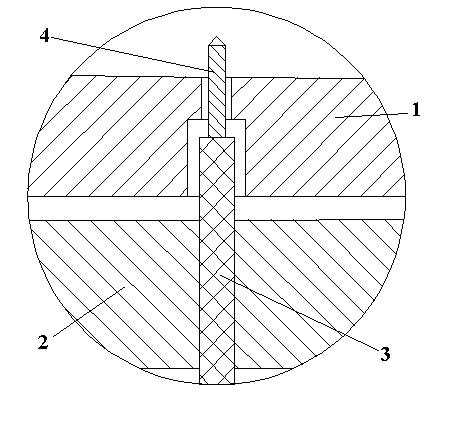
[0013] refer to figure 2 , image 3 with Figure 4 , a PCB testing device guard plate processing technology, its steps are as follows:
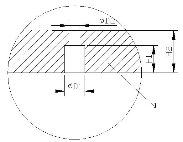
[0014] a. Open a blind hole with a diameter of D1 and a depth of H1 on the surface of the guard plate 1 facing the side of the needle planting plate 2 and corresponding to the position of the test needle 4, and D1>d1, h1
[0015] b. On the corresponding position on the reverse side of the guard plate 1 processed by the blind hole, a through hole with a diameter of D2 and a depth directly reaching the blind hole is opened, and D1>D2>d2, wherein, d2 is the maximum diameter of the needle bar 4 of the test needle, and the specific size of D2 dep...
Login to View More PUM
 Abstract
The invention relates to a processing technology of a protective plate of a PCB (Printed Circuit Board) testing device, which comprises the following steps of: a, arranging a blind hole with a diameter of D1 and a depth of H1 on a protective plate surface facing one side of a needle placing plate relative to the position of a testing needle, wherein D1>d1 and h1<H1<h2, d1 is the diameter of a needle sheath of the testing needle, h2 is the depth of the protective plate and h1 is the installation height of the needle sheath of the testing needle; and b, arranging a through hole in the reverse position of the protective plate with the processed blind hole, wherein the diameter of the through hole is D2, the depth of the through hole is equal to that of the blind hole, D1>D2>d2, and d2 is the maximum diameter of a needle rod of the testing needle. The invention meets different hole diameter requirements for the needle sheath and the needle rod of the testing needle for the protective plate, and enables the protective plate to effectively protect the testing needle, lead and correct the positioning of the testing needle, and effectively obstruct impurities such as tin balls, flux and the like from dropping on the needle sheath of the testing needle and the needle placing plate of the PCB testing device.
Description
technical field [0001] The invention relates to a process for processing a protective plate of a PCB testing device, which is suitable for other testing devices such as an ICT online tester device, an FCT function testing device, and the like. Background technique [0002] In the current PCB testing device, such as figure 1 As shown, the gap between the pinhole of the guard plate and the needle bar of the test needle is large, which cannot play the role of guiding, correcting and protecting the test needle; and sundries such as "tin beads" and "flux" are easy to fall from the gap between the pinholes of the guard plate To the test needle sleeve and the needle planting plate of the device, it will cause the test needle to short circuit or lose its elasticity, cause the test device to fail, and shorten the service life of the test needle. Therefore, how to solve the above problems is the research object of the present invention. Contents of the invention [0003] The purpo...
Claims
Login to View More Application Information
Patent Timeline
 IPC IPC(8): G01R1/02G01R1/067
Inventor沙立明何志远陈元飞
OwnerTPV ELECTRONICS (FUJIAN) CO LTD