Automatic substrate transport system and method

A technology for conveying systems and substrates, which is applied in the fields of electrical components, printed circuit manufacturing, photolithography process exposure devices, etc., can solve problems such as reducing production efficiency and prolonging manufacturing time.

Inactive Publication Date: 2010-08-04
WKK DISTRIBUTION
View PDF5 Cites 23 Cited by
  • Summary
  • Abstract
  • Description
  • Claims
  • Application Information

AI Technical Summary

Problems solved by technology

It can be seen that this practice also prolongs the manufacturing time of PCB, thereby reducing the efficiency of flow production

Method used


Image

  • Automatic substrate transport system and method
  • Automatic substrate transport system and method
  • Automatic substrate transport system and method

Examples


Embodiment Construction

[0046] The following description is intended to enable those skilled in the art to reproduce and utilize the invention and to implement it using the best mode described by the inventors. There are various modifications to the invention which will be apparent to those skilled in the art. Any of these modifications, equivalent replacements and substitutions are within the inventive idea and scope of the present invention.

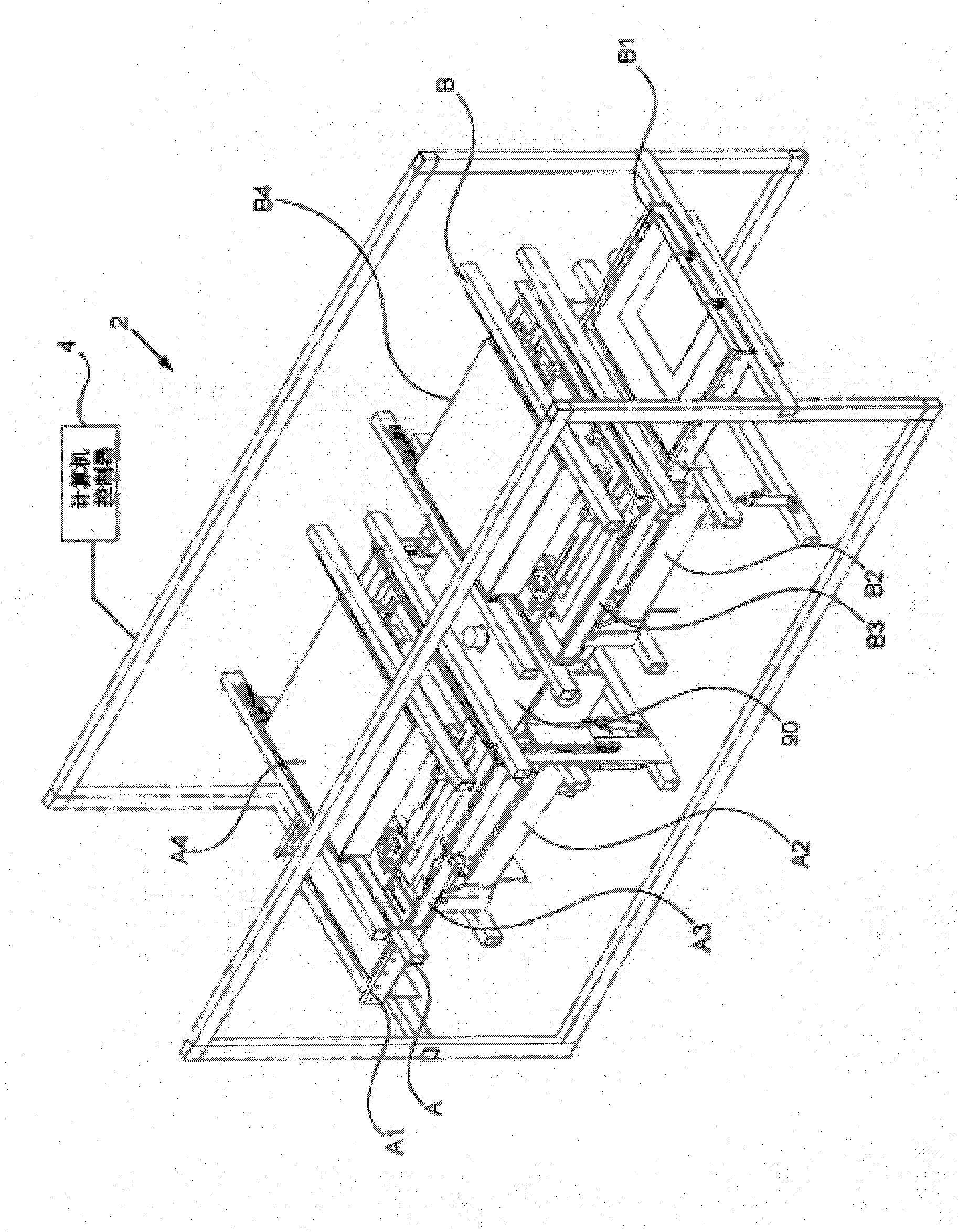
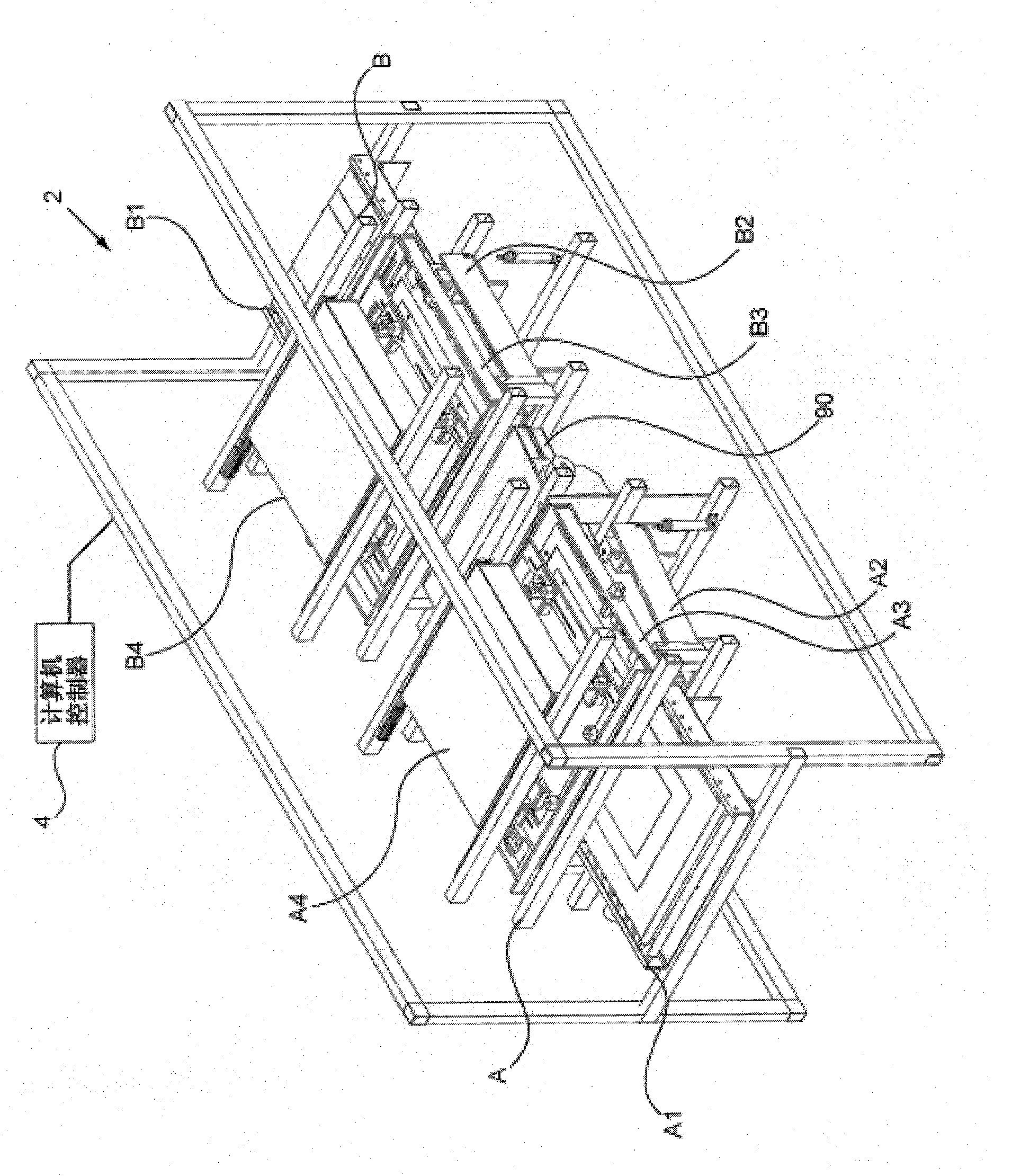
[0047] figure 1 An embodiment of the automatic substrate transfer system of the present invention is given. The automatic substrate transfer system 2 is mainly described as a specific system for processing PCB substrates. The teachings of the present invention can be applied to any substrate with photopolymerizable substances that needs to be treated with a UV exposure system. The System 2 can handle substrates ranging in size from 356mm x 356mm to 610mm x 720mm. Of course, the system can be adjusted to handle larger or smaller substrates as required. In...


PUM

PropertyMeasurementUnit
thicknessaaaaaaaaaa

Abstract

The present invention provides an automatic substrate transport system and method to transport substrate through a lamp exposure system. The system comprises a first platen, the first platen having a plurality of holes on a top surface to allow forced air to produce an air film to support a substrate; a flipper module configured to receive a substrate from the first platen, and to rotate in orderto flip the substrate, the flipper module having a top interior surface and a bottom interior surface, wherein the top and bottom interior surfaces provide a plurality of holes for froming an air film to support the substrate; and a second platen configured to receive the substrate from the flipper module, the second platen having holes on a top surface to allow forced air to produce an air film to support the substrate. The method includes use steps corresponding to the system. In the system and method, the substrate is transported substantially on a film of air, to avoid substrate scratch and transfer of thickness substance caused by contact, to further improve the flowing production efficiency of PCB.

Description

technical field [0001] The present invention relates to systems and methods for exposing lithographic materials on substrates, and more particularly, to automated substrate transport systems and methods for transporting substrates through an exposure system. Background technique [0002] Traditionally, printed circuit boards (i.e. PCBs) have required photopolymer coatings to define circuits during the manufacturing process, or protective coatings to protect the circuits after the circuits have been printed and prevent short circuits during component assembly. In both cases described, a photopolymerizable organic coating is used. Ultraviolet rays are used during the manufacture of PCBs to activate the polymerization of coating substances, ie to cure photopolymerizable substances. A common practice is that the substrate, also known as the panel, is exposed in an ultraviolet exposure system for about a few seconds to a minute. Substances in exposed areas of the plate will cur...

Claims


Application Information

Patent Timeline
Patent Type & Authority Applications(China)
IPC IPC(8): G03F7/20H05K3/00
CPCH05K13/0061
Inventor 莱昂内尔·弗尔伍德格瑞格·巴克斯特约韩·H·哈特拉贾·D·辛格
Owner WKK DISTRIBUTION
Why Eureka
Try Eureka