Supercharge Your Innovation With Domain-Expert AI Agents!

Radiation detector

一种放射线检测器、放射线的技术,应用在辐射强度测量、半导体器件、辐射控制装置等方向,能够解决尺寸误差、半导体元件施加、不能适当地连接半导体元件和单极板等问题,达到连接可靠性高的效果

Inactive Publication Date: 2010-08-18
HITACHI LTD
View PDF4 Cites 0 Cited by
  • Summary
  • Abstract
  • Description
  • Claims
  • Application Information

AI Technical Summary

Problems solved by technology

[0004] However, in the radiation detector of Patent Document 1, since the radiation detector is formed by stacking a plurality of components such as a common electrode plate and a semiconductor element, a dimensional error of each component is added to each of the stacked components. It is difficult to arrange a plurality of semiconductor elements at high density while strictly controlling the interval between semiconductor elements to a predetermined interval
In addition, the radiation detector of Patent Document 1 is constituted by tightening two frames with pins, so it may be difficult to uniformly apply tightening pressure to the semiconductor element, the semiconductor element and the monopolar plate may not be properly connected, and there may be excessive tightening. When mechanical stress is applied to the semiconductor element

Method used


Image

  • Radiation detector
  • Radiation detector
  • Radiation detector

Examples


Embodiment Construction

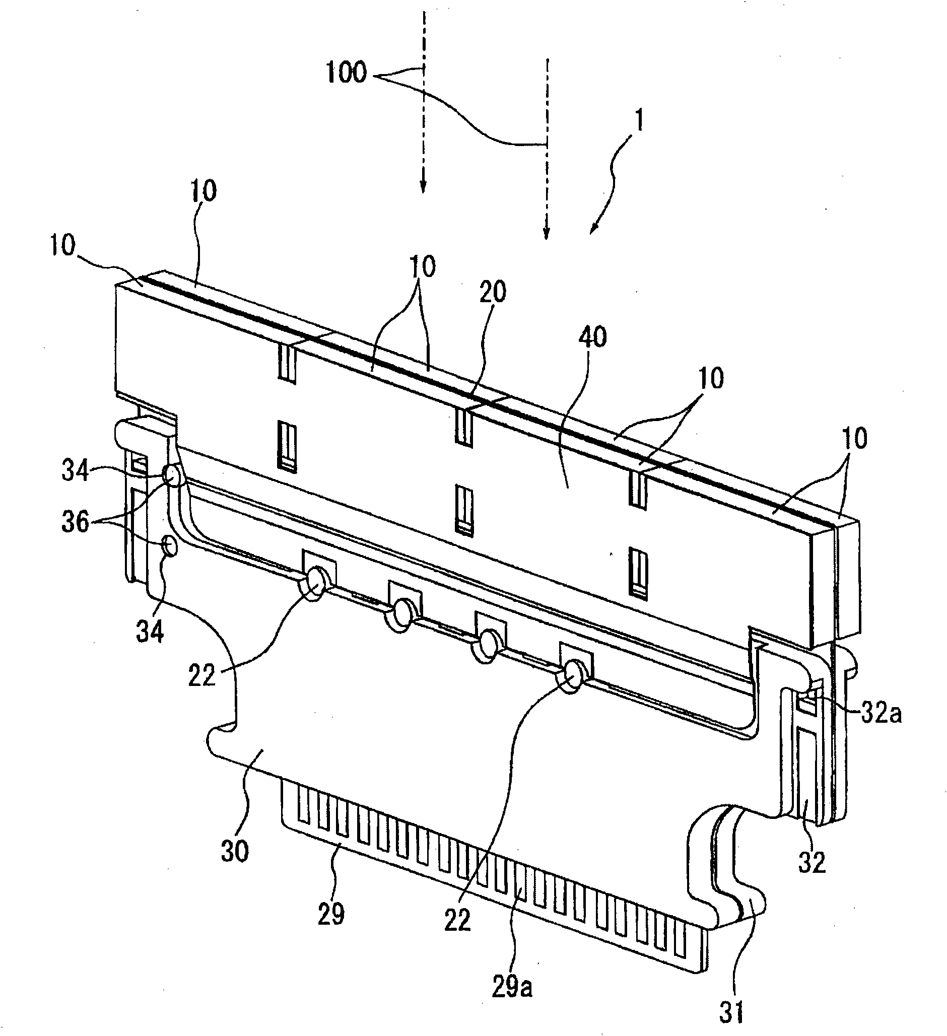
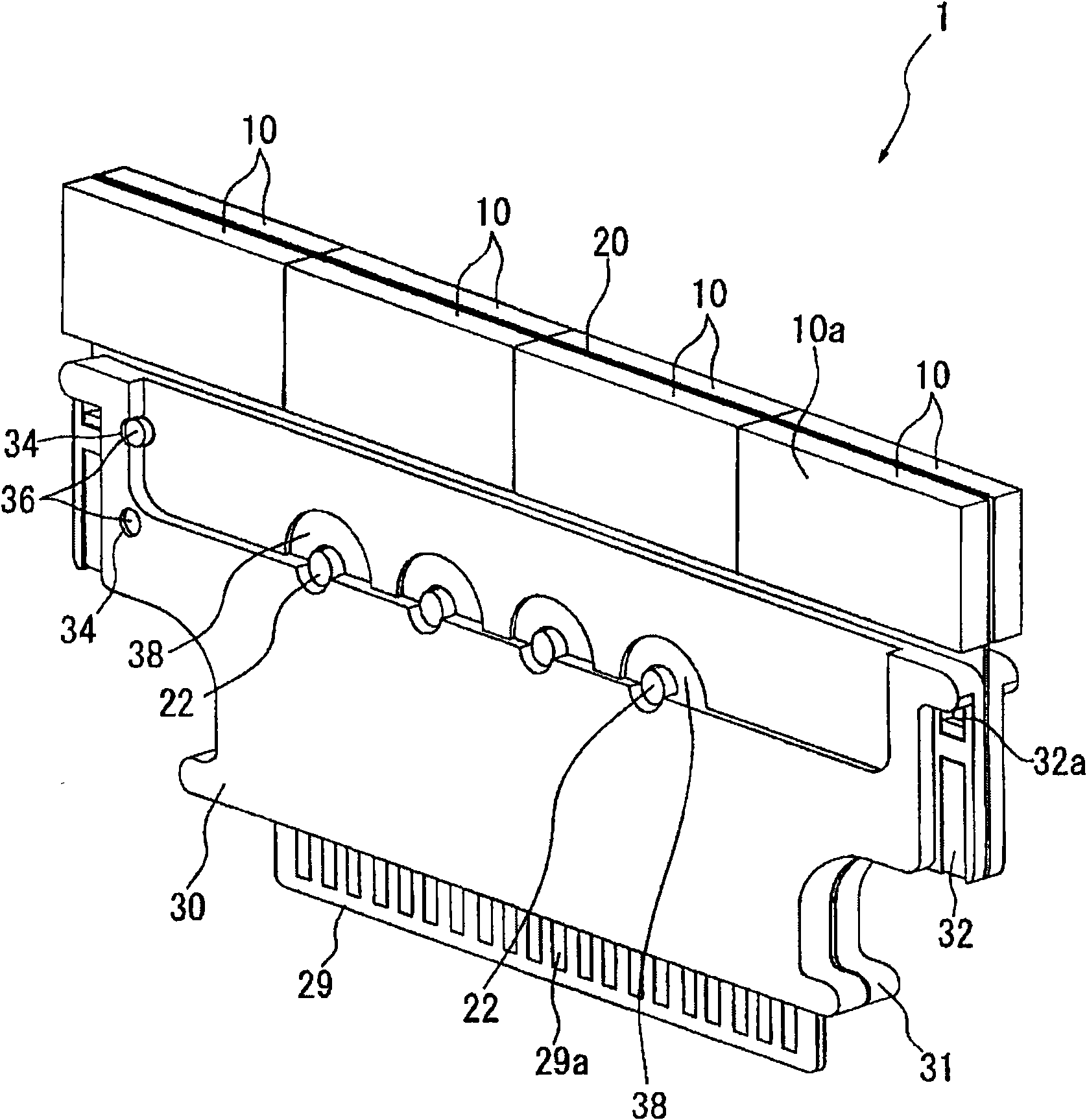
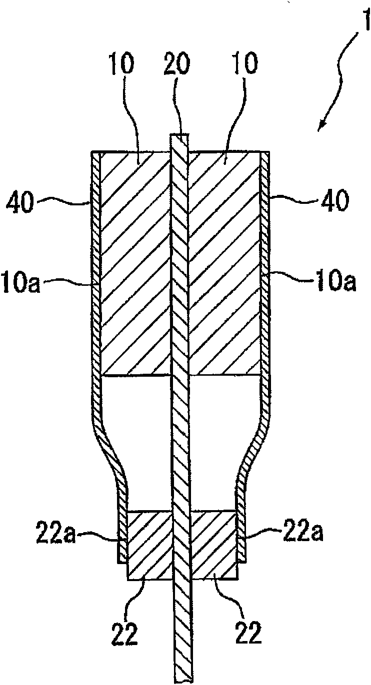
[0033] Figure 1A is a perspective view of a radiation detector according to an embodiment of the present invention, Figure 1B It is a perspective view when the flexible substrate is removed from the radiation detector of this embodiment. in addition, Figure 1C It is a schematic partial cross-sectional view of the radiation detector according to the embodiment of the present invention. Also, in Figure 1C In FIG. 2 , illustration of the card holder 30 and the card holder 31 is omitted for convenience of description.

[0034] (Outline of Configuration of Radiation Detector 1 )

[0035] The radiation detector 1 of the present embodiment is a radiation detector that detects radiation such as γ-rays and X-rays. exist Figure 1A In , radiation 100 travels from the top of the paper along the bottom. That is, the radiation 100 travels from the semiconductor element of the radiation detector 1 in a direction toward the card holder and reaches the radiation detector 1 . Also, t...


PUM


Abstract

A radiation detector includes a semiconductor element capable of detecting a radiation, a substrate on which the semiconductor element is mounted, and a flexible substrate including a connection pattern connected to an element electrode on an opposite side to the substrate of the semiconductor element. The semiconductor element is disposed on one surface of the substrate, and the flexible substrate is disposed on the opposite side to the substrate of the semiconductor element.

Description

technical field [0001] The present invention relates to radiation detectors. In particular, the present invention relates to a radiation detector used in a radiation detection device that detects radiation such as γ-rays and X-rays. Background technique [0002] As a conventional radiation detector, it is known that a plurality of common electrode plates, a plurality of semiconductor elements, and a plurality of electrode plates are arranged between two frames so that a common electrode plate, a semiconductor element, an electrode plate, a semiconductor element, and a common electrode are arranged. A radiation detector in which one frame and the other frame are fixed with pins to a laminated body stacked in the form of plates (for example, refer to Patent Document 1: US Patent No. 6,236,051). [0003] In the radiation detector described in Patent Document 1, since a pair of semiconductor elements adjacent in the lateral direction share a common electrode plate, the region w...

Claims


Application Information

Patent Timeline
Patent Type & Authority Applications(China)
IPC IPC(8): G01T1/24H01L27/144
CPCH01L31/0203H01L31/1032H01L31/0296
Inventor 柳主铉须永义则川内秀贵井上慎一高桥勋
Owner HITACHI LTD
Features
  • R&D
  • Intellectual Property
  • Life Sciences
  • Materials
  • Tech Scout
  • Unparalleled Data Quality
  • Higher Quality Content
  • 60% Fewer Hallucinations
Learn More