
Miniature image capture lens

An image and lens technology, applied in the field of wafer-level miniature image extraction lens, to achieve the effect of short track length

Active Publication Date: 2010-09-29
VISERA TECH CO LTD +1
View PDF4 Cites 9 Cited by
  • Summary
  • Abstract
  • Description
  • Claims
  • Application Information

AI Technical Summary

Problems solved by technology

[0005] Due to its glass substrate structure and repeated process limitations, wafer-level lenses have many design constraints, such as lens material, substrate thickness, lens sag height and size, optical center alignment accuracy, etc.

Method used


Image

  • Miniature image capture lens
  • Miniature image capture lens
  • Miniature image capture lens

Examples


Embodiment Construction

[0074] The implementation examples of the present invention are described below, which disclose the main technical features of the present invention, but are not intended to limit the present invention.

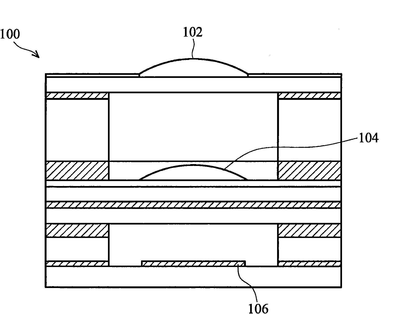
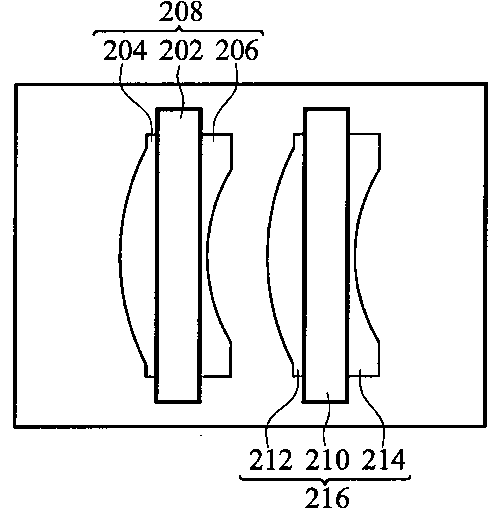
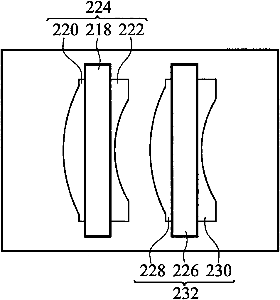
[0075] The present invention discloses a wafer-level lens system comprising two optical surfaces on opposite sides of a glass substrate. In the present invention, the two optical surfaces of the lens may be composed of different materials, one of which has a high refractive index and the other has a Low refractive index, the lens material can be ultraviolet (UV) curable polymer compound. In addition, the two-side wafer-level lens provided by the present invention has high refractive index and low refractive index respectively on the surfaces on both sides, and the wafer-level lens provided by the present invention has convex and concave surfaces on both sides respectively. to minimize optical scatter. Please note that in the present invention, different materials can be used...


PUM


Abstract

The invention relates to a miniature image capture lens, wherein an aperture diaphragm has an aperture, through which the miniature image capture lens can capture an image. A wafer scale lens system comprises a first lens group which includes a first substrate, a first surface disposed on a first side of the first substrate, a second surface disposed on a second side of the first substrate, and a second lens group which includes a second substrate, a third surface disposed on a first side of the second substrate, and a fourth surface disposed on a second side of the second substrate, wherein the first surface, the second surface, the third surface and the fourth surface are aspherical, one of the first surface and the second surface, and one of the third surface and the fourth surface have a high refraction index Nd_h and a high abbe number Vd_h, another one of the first surface and the second surface, and another one of the third surface and the fourth surface have a low refraction index Nd_l and a low abbe number Vd_l, and the miniature image capture lens meets the following conditions: Nd-h=1.58 1.62; Nd-l=1.48 1.53; Nd-l / Nd-h=0.91 0.97; Vd-h=35 45; Vd-l=25 35; and Vd-l / Vd-h=1.2 2.2, wherein one of the first and second surfaces is convex shaped and another one of the first and second surfaces is concave shaped, and one of the third and fourth surfaces is convex shaped and another one of the third and fourth surfaces is concave shaped.

Description

technical field [0001] The invention relates to a lens system, in particular to a wafer-level miniature image capture lens. Background technique [0002] Due to the development of solid-state image capture units, such as charge-coupled devices (CCD), CMOS sensors, or similar devices, image devices mounted on mobile phones or personal computers are becoming more and more popular. In addition, the image pickup lens disposed on the image element needs to be further miniaturized. [0003] However, despite the above-mentioned requirements, the miniaturization of the traditional image capture lens has encountered a bottleneck, because the above-mentioned lens is a true three-dimensional (3-D) structure, the miniaturization is quite difficult, and the Sensors also need to be miniaturized. This technique makes it difficult to precisely control the lateral movement and tilt of each lens surface, and it is also difficult to manipulate the tiny lenses during the manufacturing process...

Claims


Application Information

Patent Timeline
Patent Type & Authority Applications(China)
IPC IPC(8): G02B13/00
CPCG02B13/0085G02B13/003G02B9/04G02B13/006
Inventor 张维中邓兆展
Owner VISERA TECH CO LTD
Learn More