Semiconductor device and manufacturing method thereof
A manufacturing method, semiconductor technology, applied in the direction of semiconductor/solid-state device manufacturing, semiconductor devices, semiconductor/solid-state device components, etc., can solve the problem of reducing the dielectric strength of semiconductor modules, and achieve the effect of preventing the reduction of dielectric strength
- Summary
- Abstract
- Description
- Claims
- Application Information
AI Technical Summary
Problems solved by technology
Method used
Image

Examples
Embodiment approach 1
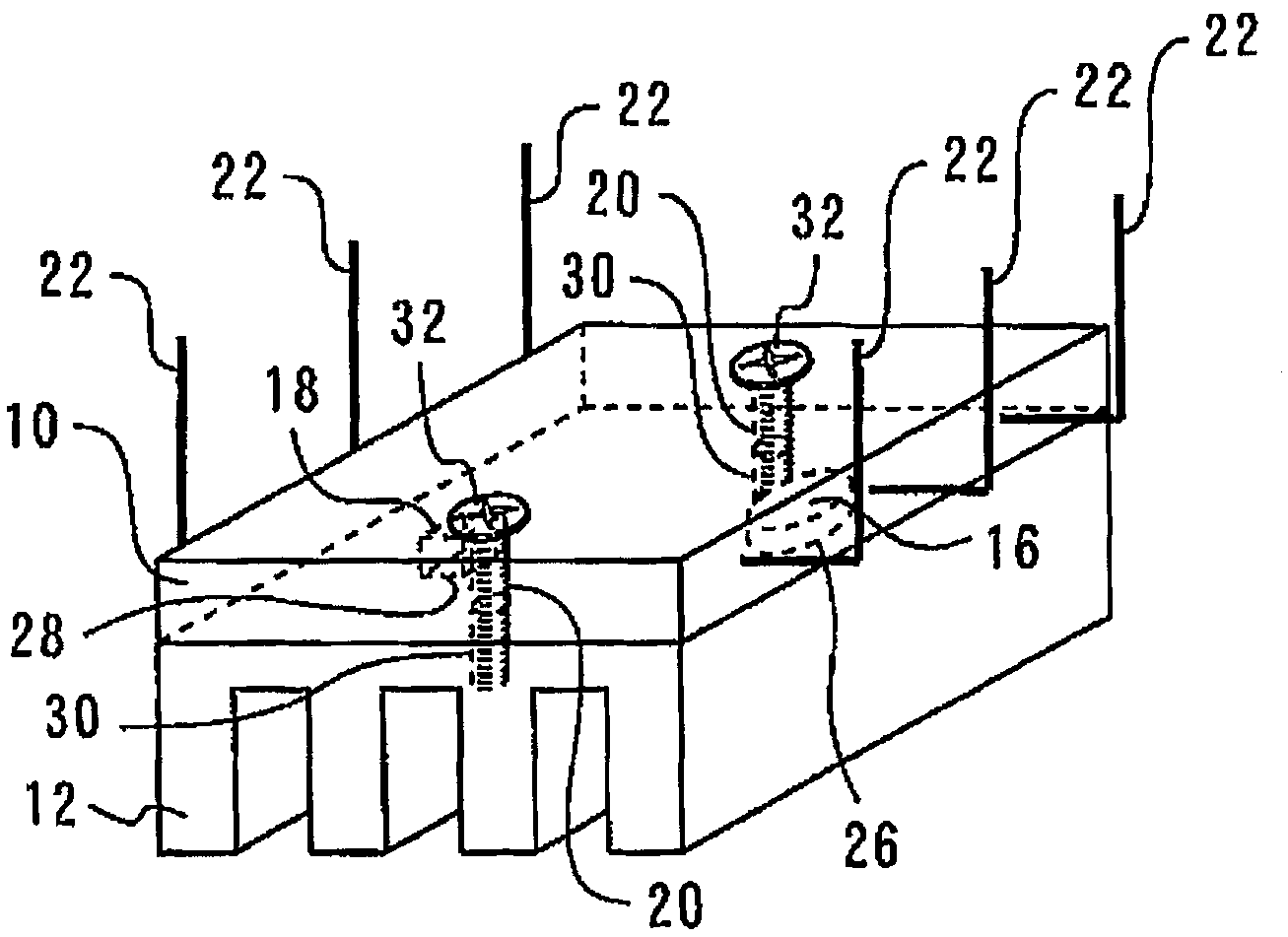
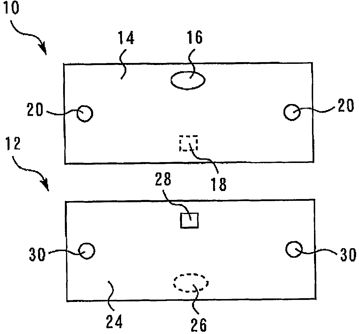
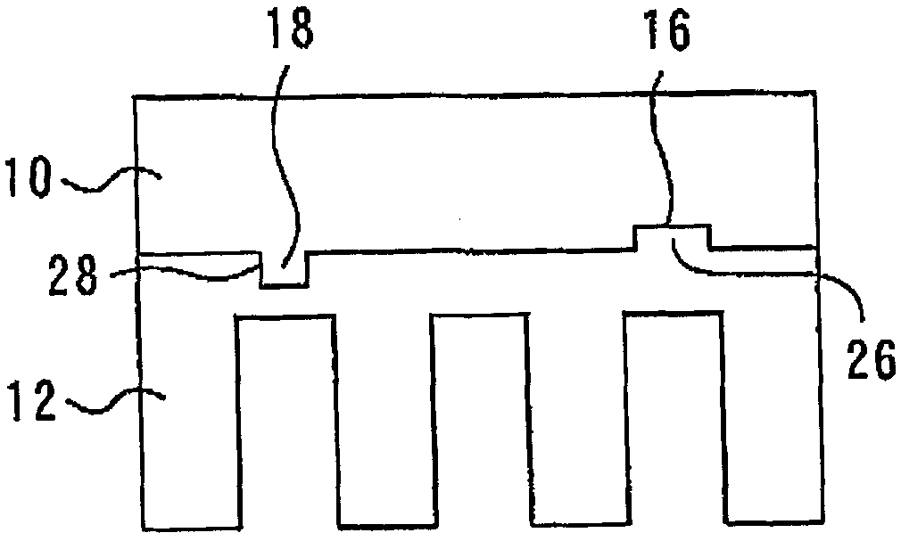
[0025] Hereinafter, the structure of the semiconductor device according to Embodiment 1 will be described. figure 1 It is a perspective view showing the semiconductor device of Embodiment 1. figure 2 It is a plan view showing the junction surface of the semiconductor module and the heat sink of Embodiment 1. image 3 It is a cross-sectional view of the semiconductor module and the heat sink of the semiconductor device according to Embodiment 1 at the fitting portion.
[0026] The semiconductor device of this embodiment includes a semiconductor module 10 and a heat sink 12 . A concave cylindrical fitting portion (first fitting portion) 16 and a convex square prism-shaped fitting portion (second fitting portion) 18 are provided on the bonding surface 14 of the semiconductor module 10 . In addition, screw holes 20 are provided at both ends of the semiconductor module 10 . Furthermore, a plurality of leads 22 are provided on both side surfaces of the semiconductor module 10 . ...
Embodiment approach 2
[0040] Hereinafter, the configuration of the semiconductor device according to Embodiment 2 will be described. Figure 5 It is a perspective view showing the semiconductor device of Embodiment 2. Figure 6 It is a plan view showing the junction surface of the semiconductor module and the heat sink of Embodiment 2. Figure 7 It is a sectional view of the semiconductor module and the heat sink of the semiconductor device according to Embodiment 2 at the fitting portion.
[0041] The semiconductor device of this embodiment includes a semiconductor module 10 and a heat sink 12 . Screw holes 20 are provided at both ends of the semiconductor module 10 . In addition, a first concave fitting portion (first fitting portion) 34 and a second concave fitting portion (second fitting portion) 36 are provided on the bonding surface 14 of the semiconductor module 10 . The first concave fitting portion 34 and the second concave fitting portion 36 are larger than the screw hole 20 and are pr...
Embodiment approach 3
[0054] Hereinafter, only the difference between the structure of the semiconductor device of Embodiment 3 and Embodiment 2 will be described. Figure 9 It is a plan view showing the junction surface of the semiconductor module and the heat sink of Embodiment 3. Figure 10 It is a cross-sectional view of the semiconductor module and the heat sink of the semiconductor device according to the third embodiment at the fitting portion.
[0055] A convex fitting portion (first fitting portion) 50 and a concave fitting portion (second fitting portion) 52 are provided on the bonding surface 14 of the semiconductor module 10 . On the other hand, a concave fitting portion (third fitting portion) 54 and a convex fitting portion (fourth fitting portion) 56 are provided on the joint surface 24 of the heat sink 12 . The concave fitting portion 54 on the heat sink 12 side has a shape that fits into the convex fitting portion 50 on the semiconductor module 10 side, and has a shape that does n...
PUM
 Abstract
Description
Claims
Application Information
 - Generate Ideas
- Intellectual Property
- Life Sciences
- Materials
- Tech Scout
- Unparalleled Data Quality
- Higher Quality Content
- 60% Fewer Hallucinations
Browse by: Latest US Patents, China's latest patents, Technical Efficacy Thesaurus, Application Domain, Technology Topic, Popular Technical Reports.
© 2025 PatSnap. All rights reserved.Legal|Privacy policy|Modern Slavery Act Transparency Statement|Sitemap|About US| Contact US: help@patsnap.com