Apparatus and method for manufacturing integrated circuits from semiconductor wafers

A technology for wafer fabrication and integrated circuits, applied in the system field of advanced process control technology

Active Publication Date: 2012-02-22
TAIWAN SEMICON MFG CO LTD
View PDF0 Cites 0 Cited by
  • Summary
  • Abstract
  • Description
  • Claims
  • Application Information

AI Technical Summary

Problems solved by technology

Again, some of these distractions are effective while others are not

Method used


Image

  • Apparatus and method for manufacturing integrated circuits from semiconductor wafers
  • Apparatus and method for manufacturing integrated circuits from semiconductor wafers
  • Apparatus and method for manufacturing integrated circuits from semiconductor wafers

Examples


Embodiment Construction

[0029] The present invention discloses an advanced process control for semiconductor manufacturing, and particularly relates to a system and method for implementing multi-resolution advanced process control. Although specific embodiments are provided herein as examples to teach the general concepts of the present invention, those of ordinary skill in the art should be able to apply the concepts disclosed in the present invention to other methods and systems. Also, the present invention discussed herein includes some known structures and / or steps. Since the structures and / or steps described above are well known, they are only discussed generally as technical details. Furthermore, the repeated reference numerals in the illustrations are only used as examples and for the convenience of description, and the above repeated reference numerals do not represent the combination of features and methods in the illustrations.

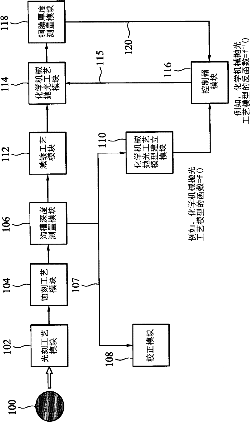
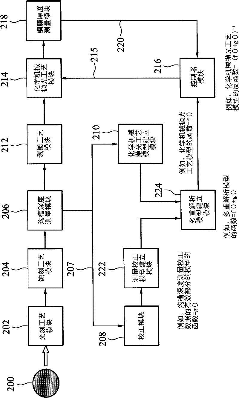
[0030] figure 1 Depicted is a portion of a well-known proce...


PUM


Abstract

The present invention provides a device and method for manufacturing an integrated circuit from a semiconductor wafer. The method includes: performing a first process on the above-mentioned semiconductor wafer; obtaining first measurement data to indicate the correctness of the executed first process; using the first A measurement data for generating measurement correction data, wherein the measurement correction data includes valid parts and invalid parts; removing the invalid part of the measurement correction data, and modeling the effective part of the measurement correction data with a measurement correction model; combining the measurement correction model with the first A first process model of a process for generating multiple analytical models, wherein the first process model models the input-output relationship of the first process; and analyzing the responses of the multiple analytical models and the second measurement data for controlling the second process effectiveness. The present invention is used to increase the control effectiveness of a controller module for advanced process control.

Description

technical field [0001] The present invention relates to an advanced process control (Advanced Process Control, APC) for integrated circuit manufacturing, in particular to a system and method for realizing the advanced process control technology of multiple analysis. Background technique [0002] Advanced process control has become an indispensable technology in semiconductor fabrication facilities (fabs), which can improve device yield and reliability at low cost. Important basic principles of advanced process control include integrated metrology, fault detection, classification, and run-to-run control. Advanced process control helps reduce process variation and production costs. The key to effective advanced process control is that the measuring instrument can measure the critical parameters within an acceptable timeframe. In addition, methods must be provided for advanced process control to analyze and interpret the measured data. In fact, advanced process control requi...

Claims


Application Information

Patent Timeline
Patent Type & Authority Patents(China)
IPC IPC(8): H01L21/66H01L21/00
CPCH01L22/12H01L22/20G05B19/41875Y02P90/02
Inventor 曾衍迪宋金宁蔡柏沣牟忠一
Owner TAIWAN SEMICON MFG CO LTD
Why Eureka
Try Eureka