Method for measuring cavity surface temperature of semiconductor laser

A temperature measurement and semiconductor technology, which is applied in the field of semiconductor laser cavity surface temperature measurement, can solve problems affecting laser performance and detection effect, etc.

Active Publication Date: 2010-10-20
INST OF SEMICONDUCTORS - CHINESE ACAD OF SCI
View PDF0 Cites 10 Cited by
  • Summary
  • Abstract
  • Description
  • Claims
  • Application Information

AI Technical Summary

Problems solved by technology

[0003] As an active device, a semiconductor laser needs to meet several conditions for its temperature measurement in its working state: First, it needs to ...

Method used


Image

  • Method for measuring cavity surface temperature of semiconductor laser
  • Method for measuring cavity surface temperature of semiconductor laser
  • Method for measuring cavity surface temperature of semiconductor laser

Examples


Embodiment Construction

[0030] Example description: common 808nm wavelength edge emitting laser cavity surface temperature measurement.

[0031] in:

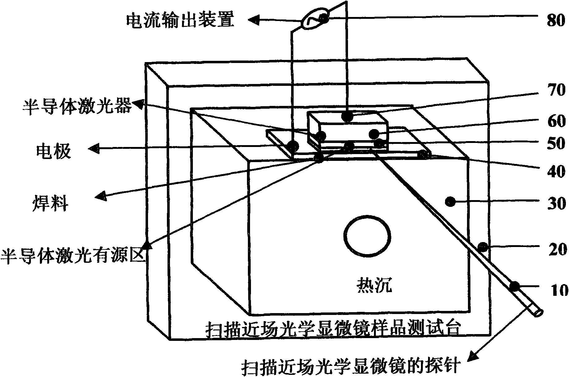
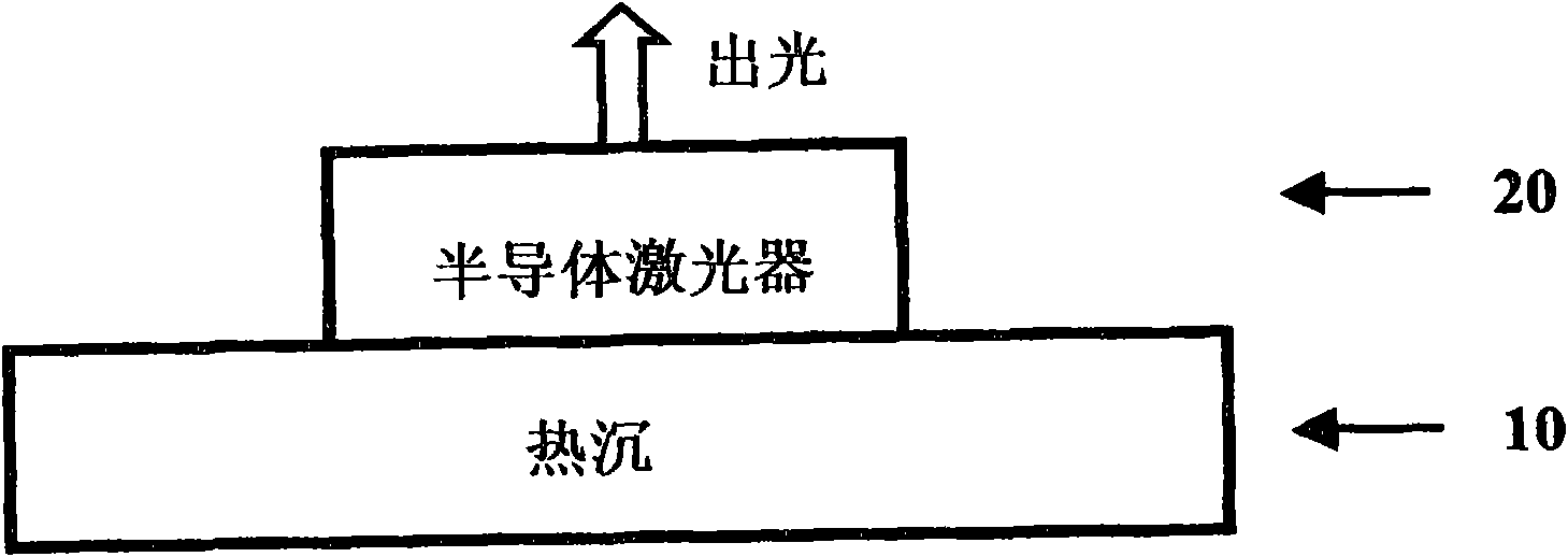
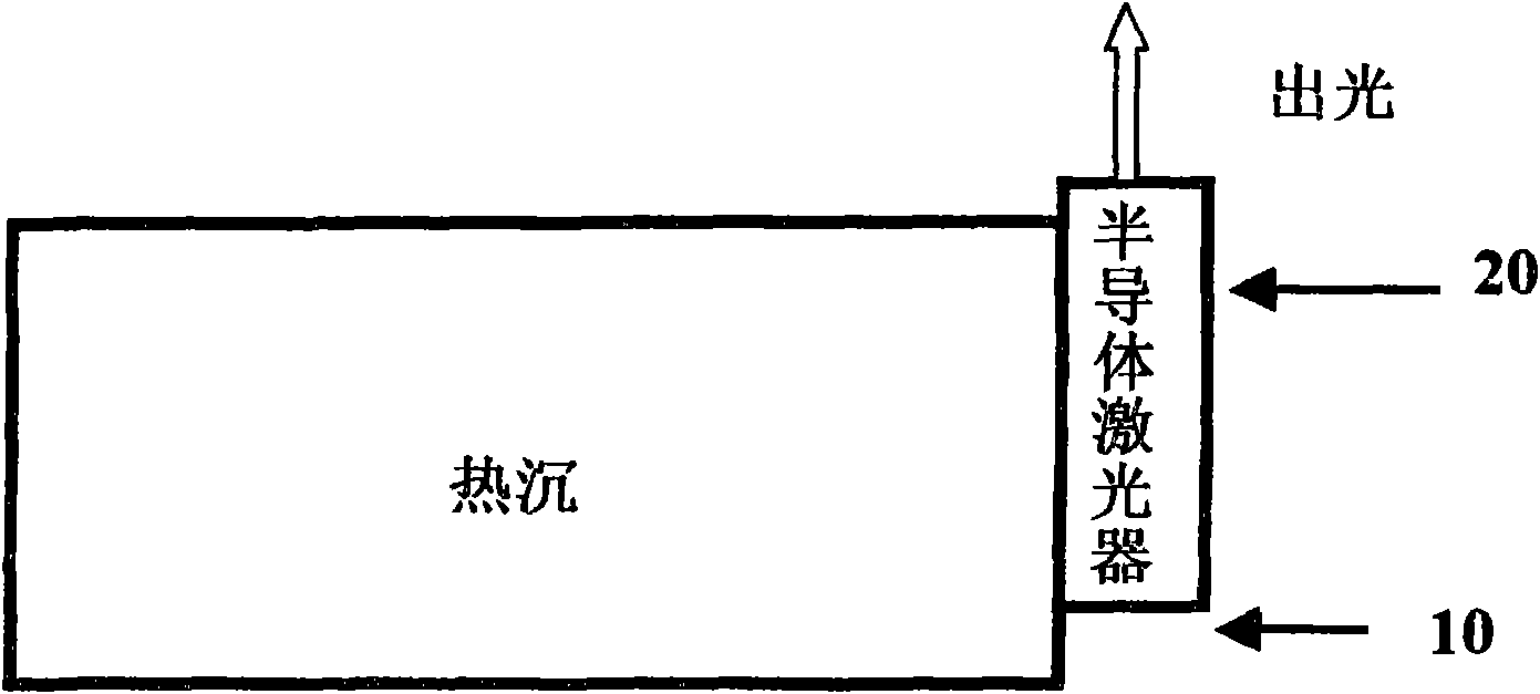
[0032] (1) Install the semiconductor laser 60 on the heat sink 30, and lead out the electrode 70; the heat sink 30 adopted in this example is a copper heat sink, and there is a circular through hole on the copper heat sink 30 for fixing. The copper heat sink has the faces with circular holes as the upper and lower sides of the heat sink 30, and the other faces are the sides of the heat sink 30 (see figure 1 ). This test method is suitable for surface-emitting semiconductor lasers 60 and edge-emitting semiconductor lasers 60. In order to enable the heat sink 30 with semiconductor lasers 60 to be easily installed on the scanning near-field optical microscope sample test stand 20, for surface-emitting and edge-emitting There are differences in the position where the semiconductor laser is mounted on the heat sink. For the surface-emitting semiconductor...


PUM


Abstract

The invention relates to a method for measuring cavity surface temperature of a semiconductor laser by using a scanning near-field optical microscope, which comprises the following steps of: installing the semiconductor laser on a heat sink, and leading out an electrode; testing parameters of the semiconductor laser; fixing the heat sink on a sample test table of the scanning near-field optical microscope; connecting an electrode with a current output end of a current output device; placing a probe of the scanning near-field optical microscope above a light emergent cavity surface of the semiconductor laser; enabling the semiconductor laser to be close to the probe of the scanning near-field optical microscope to be in a non-contact working state; determining the scanning range of an active region including the semiconductor laser according to the characteristic dimension of the semiconductor laser; scanning to obtain a feature image under the condition of no current injection; injecting a constant current to obtain a feature image and a near field light spot image of the light emergent cavity surface of the semiconductor laser; comparing the feature images before and after the current is injected, calculating the difference value of the feature change; and calculating corresponding temperature change according to coefficients of thermal expansion of various materials in the semiconductor laser.

Description

technical field [0001] The invention relates to a method for measuring the cavity surface temperature of a semiconductor laser, which has the characteristics of simple and convenient measurement of the cavity surface temperature of the semiconductor laser, and belongs to the technical field of semiconductor devices. Background technique [0002] Semiconductor lasers are widely used in commercial, industrial, medical, military and other fields, and their main advantages are small size, long life, good stability, high energy efficiency, and low cost. In recent years, with the development of industry, medical treatment and military affairs, the requirements for the output power of lasers have been continuously improved. For high-power semiconductor lasers, the optical load and heat load on the laser cavity surface are very large, which causes the laser cavity surface to degrade and affects the performance and life of the laser. Therefore, studying the temperature characteristic...

Claims


Application Information

Patent Timeline
IPC IPC(8): G01K5/48G01R31/26
Inventor 饶岚宋国峰汪卫敏陈良惠
Owner INST OF SEMICONDUCTORS - CHINESE ACAD OF SCI
Why Eureka
Try Eureka