Optical scanning device and image forming apparatus

a scanning device and image forming technology, applied in the field of optical scanning devices, can solve the problems of difficult manufacturing of such, power change, and design value variation of optical characteristics,

Active Publication Date: 2007-09-13
RICOH KK
View PDF26 Cites 60 Cited by
  • Summary
  • Abstract
  • Description
  • Claims
  • Application Information

AI Technical Summary

Benefits of technology

[0020]It is an object of the present invention to at least

Problems solved by technology

Therefore, there is a problem in which the optical characteristics, in particular, power, are changed from design values and a beam spot diameter, which is a diameter of a light spot at the time of light-gathering of light beams on a plane to be scanned, is varied according to environmental variations.
A change in wavelength in the light source may cause a change in characteristics due to chromatic aberration of the optical system for use in the optical scanning device, and this change in characteristic also may cause a variation in beam spot diameter.
Since a curved reflecting surface is included, manufacturing of such is not necessarily easy, and a further improvement has to be made in view of cost reduction of the optical scanning device.
Furthermore, in general, the diffracting surface requires microfabrication technology, and also requires extremely high accuracy.
As evident from FIG. 14B, t

Method used


Image

  • Optical scanning device and image forming apparatus
  • Optical scanning device and image forming apparatus
  • Optical scanning device and image forming apparatus

Examples


first embodiment

[0073]A specific configuration of the respective components forming the optical system of the optical scanning device depicted in FIG. 2 is as follows.

Light Source:

[0074]The semiconductor laser 1 as a light source has a designed light-emitting wavelength of 785 nanometers. When the temperature increases by 1 degree Celsius with respect to the normal temperature of 25 degrees Celsius, the light-emitting waveform is shifted by 0.25 nanometers to a long wavelength side. As for the mode hop, a wavelength change of 0.8 nanometers is assumed, as mentioned above.

Coupling Lens:

[0075]The coupling lens 2 is a resin-made lens having the power diffracting surface as mentioned above, and is disposed so as to have a focal length of 13.952 millimeters and a function for conversion to a weak diverged light beam. One side surface of the coupling lens 2 is aspheric. With this aspheric surface, wave aberration of the light beam converted to have a desired cross-section shape is sufficiently corrected...

second embodiment

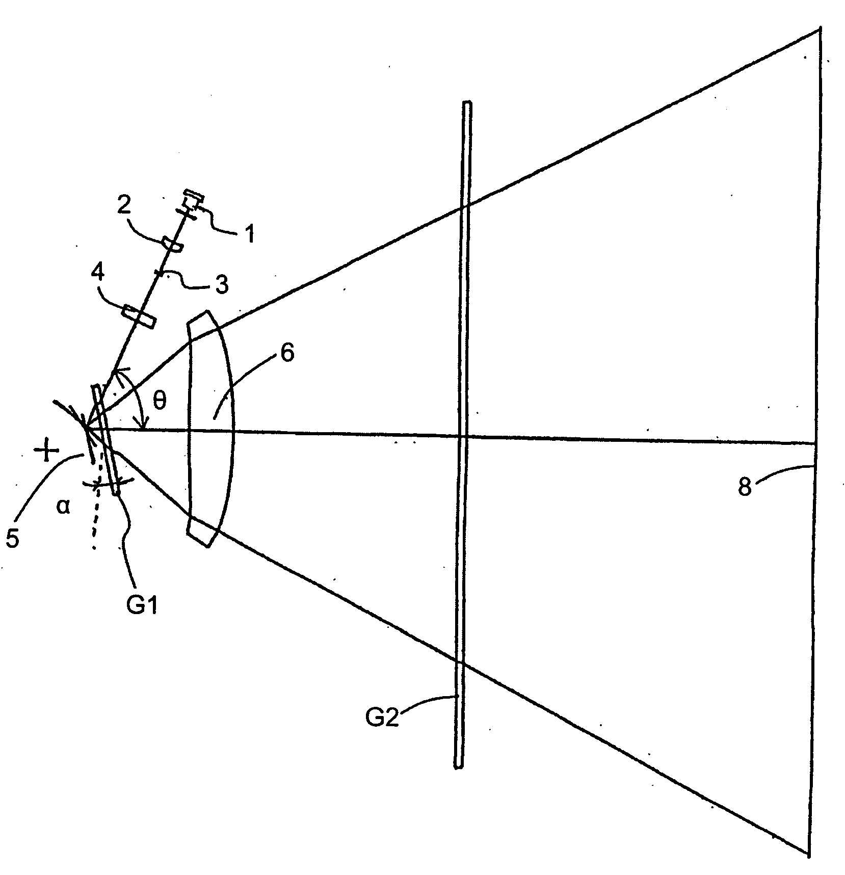
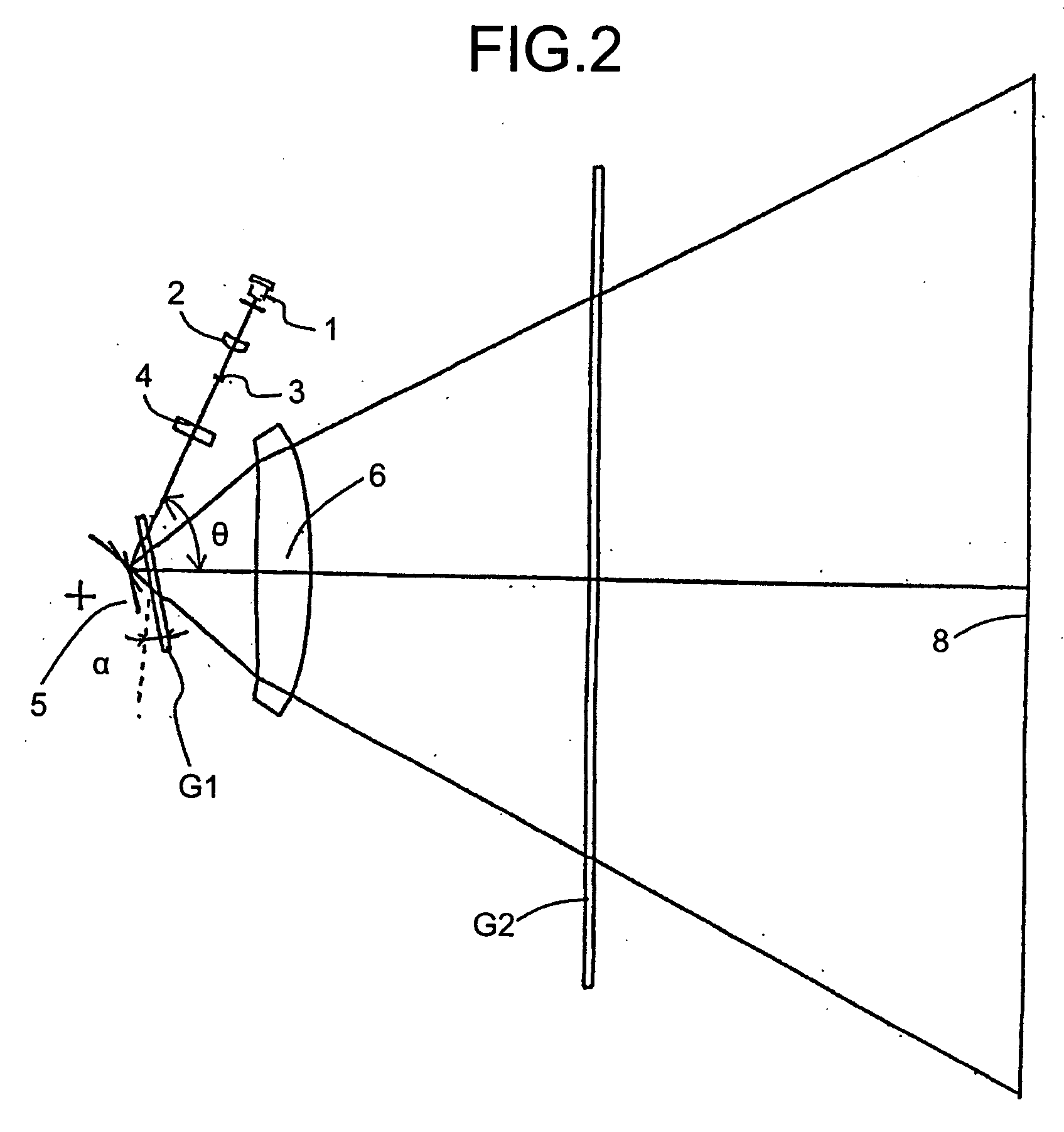
[0087]FIG. 4 is a configuration diagram that depicts an arrangement of optical elements of the optical scanning device according to the In FIG. 4, 1 denotes a semiconductor as a light source, 2 denotes a coupling lens as a first optical element, 3 denotes an aperture, 4 denotes an anamorphic optical element as a second optical element, 5 denotes a polygon mirror, which is a rotational polygon mirror as an optical deflector, 6 denotes a scanning optical system as a third optical element, and 8 denotes a surface to be scanned. Also, G1 denotes a sound-shielding glass for shielding a window of a sound-shielding housing (not shown) that has accommodated therein the polygon mirror 5, whilst G2 denotes a dustproof glass provided at a deflected-light-beam ejecting unit of a housing having accommodating therein the optical system of the optical scanning device depicted in FIG. 4.

[0088]A diverged light beam emitted from the semiconductor laser 1 is converted by the coupling lens 2 to a ligh...

third embodiment

[0132]Furthermore, the resin-made scanning lens can be easily adopted for an aspheric surface and a free surface. As initial characteristics, excellent optical characteristics including a small beam spot diameter can be ensured. With such configuration of each component optical characteristics including temperature characteristics, which have been solely problematic, can be improved.

[0133]As has been explained, the power of the entire surface is distributed over the refractive portion of the refractive surface 2b, thereby making an optical element resistant to eccentricity between surfaces. However, what is most desirable is that the power of the diffracting surface 2a is 0, specifically, P1=−P2. With this, it is possible to provide an optical scanning device with less deterioration in beam spot diameter even if the diffracting surface 2a is eccentric with respect to the refractive surface 2b.

[0134]Also, if the diffracting surface 2 has a stepwise configuration, a forming scheme c...


PUM


Abstract

An optical scanning device includes a first optical element that converts a cross-section shape of a light beam from a semiconductor laser to a desired shape; a second optical element that guides the light beam output from the first optical element to an optical deflector that deflects the light beam; and a third optical element that gathers the light beam deflected by the optical deflector onto a surface to be scanned to form a light spot thereby optically scanning the surface. At least one of the first optical element, the second optical element, and the third optical element includes a resin-made lens, at least one of the resin-made lenses has a power diffracting surface, and a surface shape of at least one of power diffracting surfaces is formed so that a power of a diffracting portion and a power of a refractive portion are cancelled out.

Description

CROSS-REFERENCE TO RELATED APPLICATIONS[0001]The present document incorporates by reference the entire contents of Japanese priority documents, 2006-067323 filed in Japan on Mar. 13, 2006, and Japanese priority document, 2006-074457 filed in Japan on Mar. 17, 2006.BACKGROUND OF THE INVENTION[0002]1. Field of the Invention[0003]The present invention generally relates to an optical scanning device that can be employed in an image forming apparatus. The present invention specifically relates to a lens in an optical scanning device.[0004]2. Description of the Related Art[0005]Conventionally, optical scanning devices have been widely used in image forming apparatuses, such as optical printers, digital copiers, or optical plotters. In recent years, low-price optical scanning devices less prone to be influenced by environmental fluctuations and configured to support formation of high-definition images have been desired.[0006]When various lenses for use in an optical scanning device are for...

Claims


Application Information

Patent Timeline
IPC IPC(8): G02B26/08
CPCG02B26/124G02B26/125G02B27/4283G02B27/0037G02B27/4227G02B27/0031
Inventor SAKAI, KOHJIHAYASHI, YOSHINORIICHII, DAISUKE
Owner RICOH KK
Why Eureka
Try Eureka