

Slot filling method in multilayer integrated circuit
A filling method and integrated circuit technology, which is applied in the manufacture of circuits, electrical components, semiconductors/solid-state devices, etc., and can solve problems such as inability to remove photoresist and pollution of photoresist processes
- Summary
- Abstract
- Description
- Claims
- Application Information
AI Technical Summary
Problems solved by technology
Method used
Image

Examples
Embodiment Construction
[0027] The filling method of groove in multilayer integrated circuit of the present invention comprises the steps:
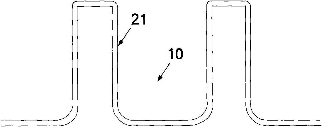
[0028] At the beginning, the surface of the silicon wafer has just etched a groove 10, and a layer of silicon dioxide (not shown) is thermally oxidized on the surface of the silicon wafer with the groove 10. The thickness of this layer of silicon dioxide is 50 ~ between.
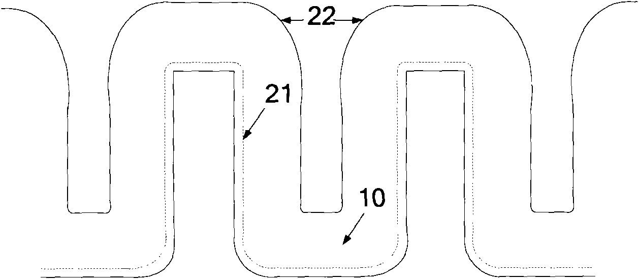
[0029] Step 1, see Figure 2a , deposit a layer of silicon dioxide on the surface of the silicon wafer with the trench 10, this layer of silicon dioxide is a pad layer 41, not doped with p-type or n-type impurities, with a thickness of 500~ between.
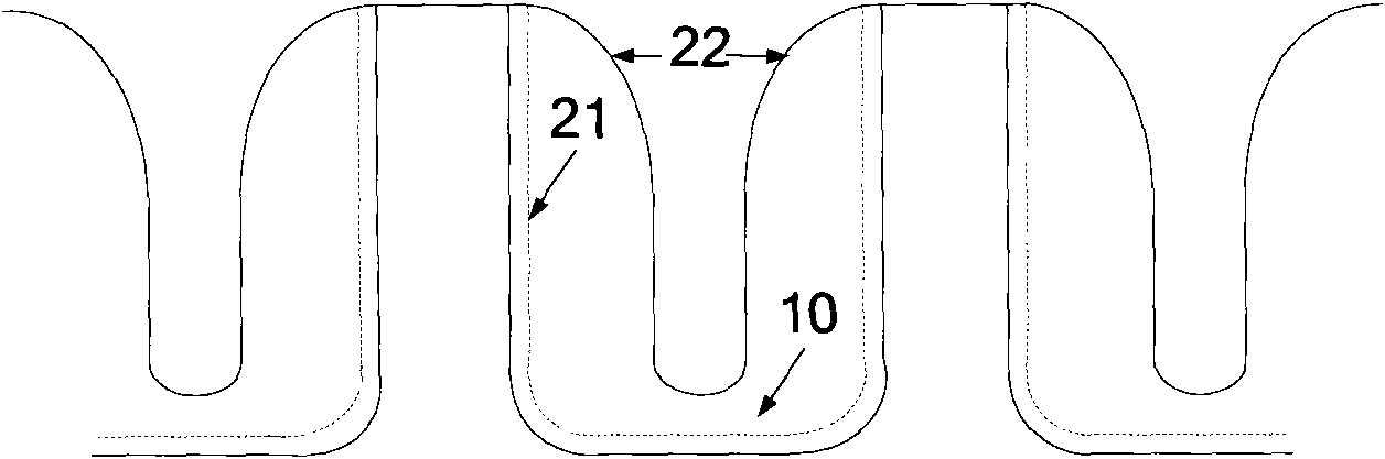
[0030] Step 2, see Figure 2b , and then deposit a layer of silicon dioxide doped with p-type or n-type impurities on the surface of the silicon wafer, with a thickness of 5000~ In between, this layer of silicon dioxide fills the trench 10 on the one hand, and serves as a material for the first layer of interlayer dielectric 42 on the oth...
PUM
 Abstract
Description
Claims
Application Information