Substrate structure and manufacturing method thereof

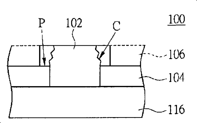
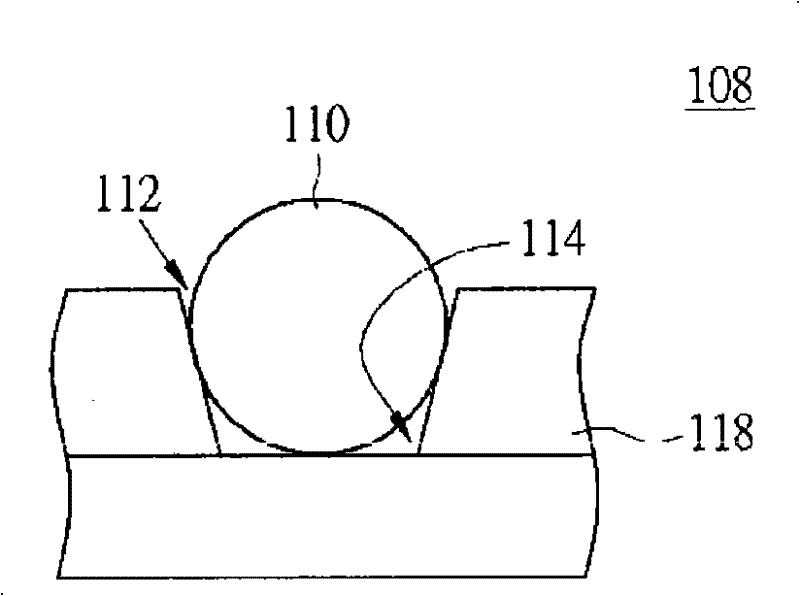
A manufacturing method and substrate technology, which are applied in the manufacture of semiconductor/solid-state devices, electrical components, and electrical solid-state devices, etc., can solve problems such as the inability to fill the corners 114 and affecting the electrical connection quality of the solder balls 110.

Active Publication Date: 2012-05-30
ADVANCED SEMICON ENG INC
View PDF0 Cites 0 Cited by
  • Summary
  • Abstract
  • Description
  • Claims
  • Application Information

AI Technical Summary

Problems solved by technology

The existing substrate structure 108 has a solder ball 110 and an insulating layer 118. Because the surface tension of the corner 114 in the insulating layer opening 112 is relatively high, the solder ball 110 of the substrate structure 108 cannot completely fill the corner 114.
In this way, the electrical connection quality of the solder ball 110 will also be affected

Method used


Image

  • Substrate structure and manufacturing method thereof
  • Substrate structure and manufacturing method thereof
  • Substrate structure and manufacturing method thereof

Examples


Embodiment Construction

[0025] Please refer to figure 2 , which shows a substrate structure according to a preferred embodiment of the present invention. In this embodiment, a substrate structure 100 suitable for flip-chip chips is taken as an example for illustration. The substrate structure 200 includes a base material 202 , a first insulating layer 204 , a conductive portion 206 , a second insulating layer 208 , a first seed layer 210 and a conductive layer 212 .

[0026] The substrate 202 has a first circuit layer 214 and a second circuit layer 216 respectively formed on opposite sides of the substrate 202 and the substrate 202 also has a via (Via) 220 as the first circuit layer 214 and the second circuit layer 216 electrical connection channels. In addition, the first insulating layer 204, such as green paint, is formed on the first circuit layer 214, the first insulating layer 204 has a first insulating layer opening 224, and the first insulating layer opening 224 is on the outer surface of ...


PUM


Abstract

The invention provides a substrate structure and a manufacturing method thereof. The substrate structure comprises a base material, a first insulating layer, a conductive portion, a second insulating layer, a seed layer and a conducting layer, wherein the base material comprises a first line layer and a second line layer which are respectively formed on the two opposite surfaces of the substrate;the first insulating layer is formed on the first line layer and is provided with a first insulating layer opening, and the first insulating layer opening exposes a first opening on the outer surfaceof the first insulating layer; the conductive portion is formed at the first insulating layer opening, is electrically connected with a chip and is enclosed by the edge of the first opening; the second insulating layer is formed on the second line layer and is provided with a second insulating layer opening; the seed layer is formed in the second insulating layer opening; and the conducting layeris formed on the seed layer and is electrically connected with a circuit board.

Description

technical field [0001] The present invention relates to a substrate structure and a manufacturing method thereof, and in particular to a substrate structure suitable for a flip-chip chip and a manufacturing method thereof. Background technique [0002] Please refer to Figure 1A , which shows a schematic diagram of the existing substrate structure. A conventional substrate structure, such as a substrate structure 100 suitable for a flip-chip chip, has a base material 116 , a conductive portion 102 and an insulating layer 104 . The conductive portion 102 is used to electrically connect with a chip (not shown), such as a flip-chip chip. Part of the conductive portion 102 is in contact with the insulating layer 104 , such as a solder mask. Figure 1A The dry film 106 is formed before the conductive part 102 is formed in order to define the range of the conductive part 102 . And it is removed after the conductive portion 102 is formed to form the substrate structure 100 . Dur...

Claims


Application Information

Patent Timeline
Patent Type & Authority Patents(China)
IPC IPC(8): H01L23/498H01L23/13H01L21/48
Inventor 李志成
Owner ADVANCED SEMICON ENG INC
Why Eureka
Try Eureka