Touch panel including a layered structure with first and second mesh terminal layers directly overlaid on each other and touch panel production method

a touch panel and production method technology, applied in the field of touch panels, can solve the problems of difficult to achieve a good and stable electrical connection state by such external connection terminals, and achieve the effect of improving electrical connection quality and good and stable electrical connection

Active Publication Date: 2021-06-08
JAPAN AVIATION ELECTRONICS IND LTD
View PDF26 Cites 0 Cited by
  • Summary
  • Abstract
  • Description
  • Claims
  • Application Information

AI Technical Summary

Benefits of technology

[0016]An object of the present invention is to provide a touch panel provided with an external connection terminal having electrical connection quality improved over conventional external connection terminals and a method for producing such a touch panel.
[0019]The present invention can provide a touch panel provided with a external connection terminal having improved electrical connection quality and enables good and stable electrical connection to an external circuit.
[0020]Further, a method for producing a touch panel according to the present invention can advantageously produce such a touch panel.

Problems solved by technology

However, external connection terminals in the form of a mesh of fine lines formed by printing as described above have a problem that the external connection terminals in general inevitably have a larger contact resistance than external connection terminals made of a solid film and therefore it is difficult to accomplish a good and stable electrical connection state by such external connection terminals.

Method used


Image

  • Touch panel including a layered structure with first and second mesh terminal layers directly overlaid on each other and touch panel production method
  • Touch panel including a layered structure with first and second mesh terminal layers directly overlaid on each other and touch panel production method
  • Touch panel including a layered structure with first and second mesh terminal layers directly overlaid on each other and touch panel production method

Examples


Embodiment Construction

[0032]Example embodiments of the present invention will be described below.

[0033]FIGS. 4A, 4B and 5 illustrate details of external connection terminals of one example embodiment of a touch panel according to the present invention and FIG. 6 illustrates the example embodiment of the touch panel according to the present invention with an FPC, which is an external circuit, connected with the external connection terminals.

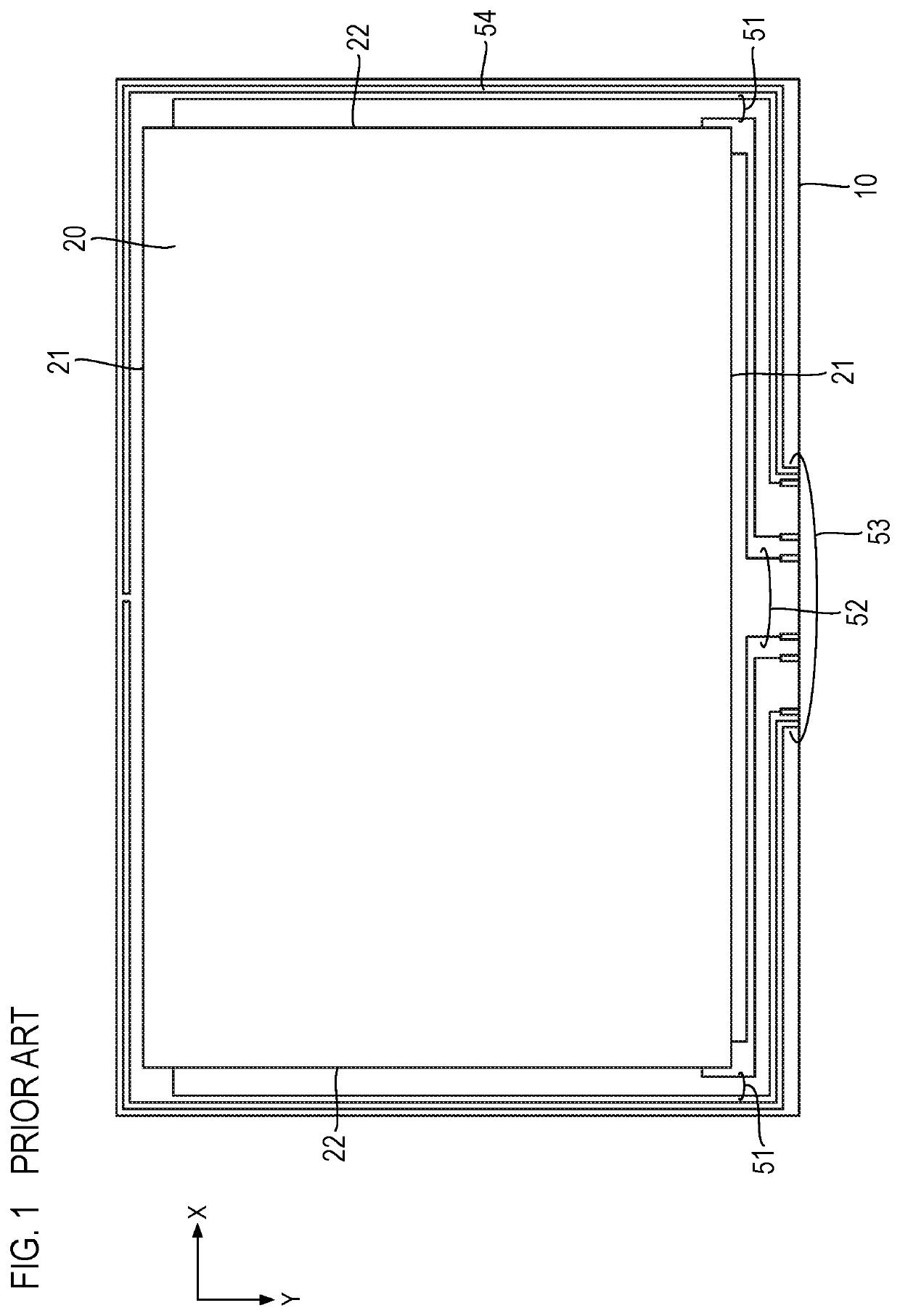
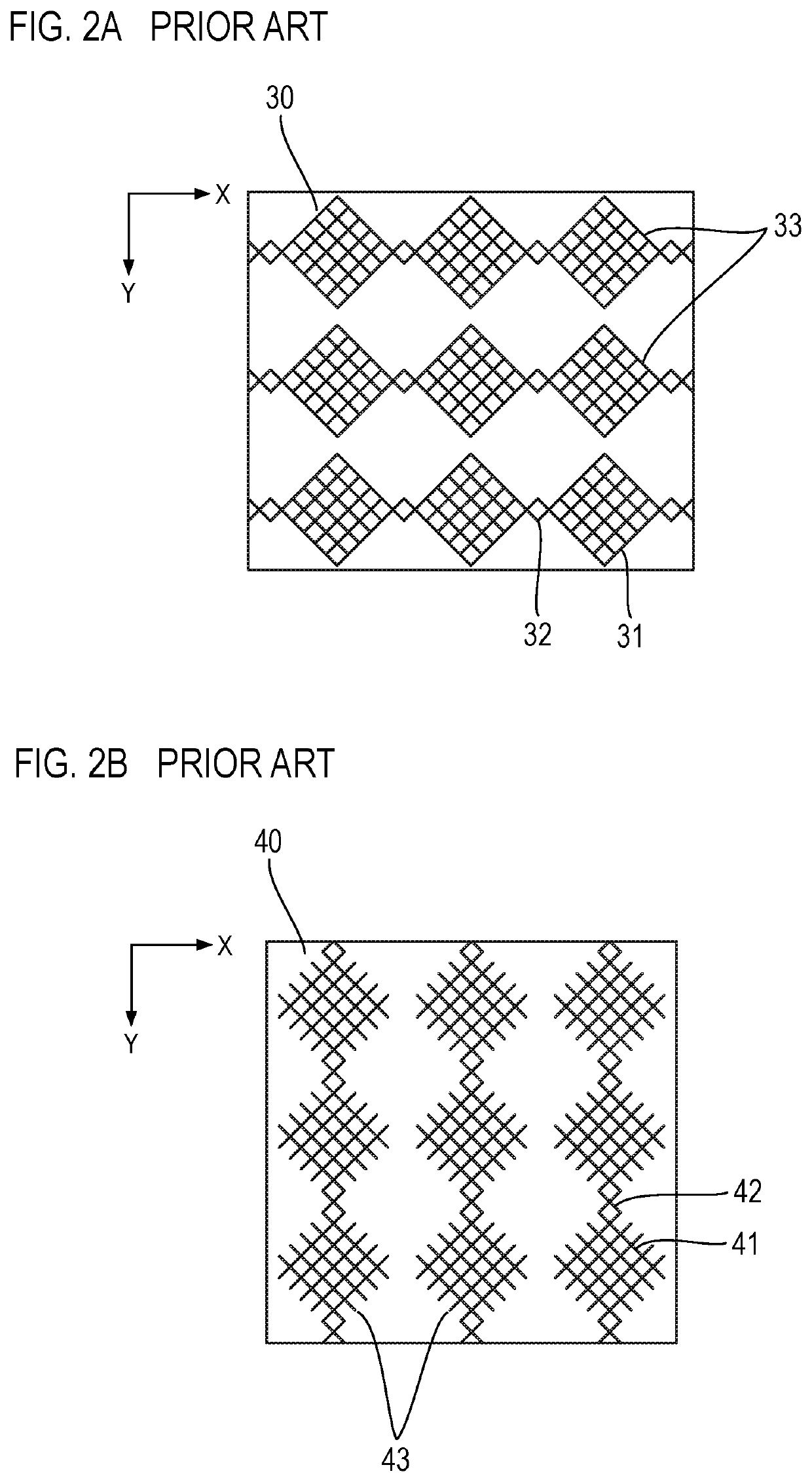
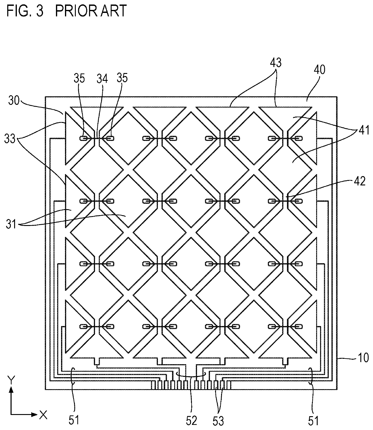
[0034]The touch panel in this example differs from the example conventional touch panel illustrated in FIG. 1 in the configuration of external connection terminals formed in an array in the center portion of one of the long sides of the substrate 10 and the configuration in the sensing region 20. The other configurations are basically the same as the configurations illustrated in FIG. 1. Note that details of the configuration in the sensing region 20 are omitted from FIG. 6.

[0035]The touch panel has a layered structure in which a first conductor layer made of a first h...


PUM

PropertyMeasurementUnit
side lengthaaaaaaaaaa
widthaaaaaaaaaa
diameteraaaaaaaaaa

Abstract

A touch panel comprises, a substrate, a layered structure formed in a sensing region defined on one side of the substrate, the layered structure including at least a first conductor layer made of a first hardened conductive ink, a second conductor layer made of a second hardened conductive ink and an insulating layer disposed therebetween, and an external connection terminal formed outside the sensing region on the one side of the substrate, wherein the external connection terminal comprises a first terminal layer made of the first hardened conductive ink and a second terminal layer made of the second hardened conductive ink, such that the first terminal layer and the second terminal layer are directly overlaid on each other.

Description

TECHNICAL FIELD[0001]The present invention relates to a touch panel that is produced using a printing process and a method for producing such a touch panel.BACKGROUND ART[0002]FIGS. 1, 2A and 2B illustrate a configuration of a capacitive touch panel described in Japanese Patent Application Laid Open No. 2017-103317 (published on Jun. 8, 2017, hereinafter referred to as Literature 1) as an example of a conventional touch panel of this type. The touch panel comprises a first conductor layer, an insulating layer, a second conductor layer, and a protective coating which are stacked in this order on a transparent substrate (substrate plate) 10. An area enclosed in a rectangular frame in FIG. 1 is a sensing region (sensor region) 20 in which sensor electrodes are located. Details of the sensor electrodes are omitted from FIG. 1.[0003]The sensor electrodes include a first sensor electrode and a second sensor electrode. The first sensor electrode is formed from a first conductor layer and t...

Claims


Application Information

Patent Timeline
Patent Type & Authority Patents(United States)
IPC IPC(8): G06F3/044B41M3/00H05K3/12
CPCG06F3/0445B41M3/006G06F3/0446H05K3/1275B41P2200/13G06F2203/04103G06F2203/04112H05K2203/0534B41F13/193G06F2203/04111
Inventor SAKAUE, AKITOSHI
Owner JAPAN AVIATION ELECTRONICS IND LTD
Why Eureka
Try Eureka