Word line-sharing contactless silicon nitride split gate type flash memory and manufacturing method thereof

A technology of split-gate flash memory and silicon nitride, which is used in semiconductor/solid-state device manufacturing, electrical components, electrical solid-state devices, etc., can solve problems such as device programming voltage reduction, and achieve device size reduction, process compatibility, and small size. Effect

Active Publication Date: 2015-01-07
SHANGHAI HUAHONG GRACE SEMICON MFG CORP
View PDF3 Cites 0 Cited by
  • Summary
  • Abstract
  • Description
  • Claims
  • Application Information

AI Technical Summary

Problems solved by technology

When traditional flash memory is moving towards higher storage density, due to structural limitations, it will face great challenges to further reduce the programming voltage of the device

Method used


Image

  • Word line-sharing contactless silicon nitride split gate type flash memory and manufacturing method thereof
  • Word line-sharing contactless silicon nitride split gate type flash memory and manufacturing method thereof
  • Word line-sharing contactless silicon nitride split gate type flash memory and manufacturing method thereof

Examples


Embodiment Construction

[0054] In order to better understand the technical content of the present invention, specific embodiments are given and described below in conjunction with the accompanying drawings.

[0055] The present invention proposes a non-contact silicon nitride split-gate flash memory and a manufacturing method thereof for sharing word lines. The obtained flash memory device can effectively reduce the area of ​​the chip while keeping the electrical isolation performance of the chip unchanged. At the same time, the problem of over-erasing can also be avoided.

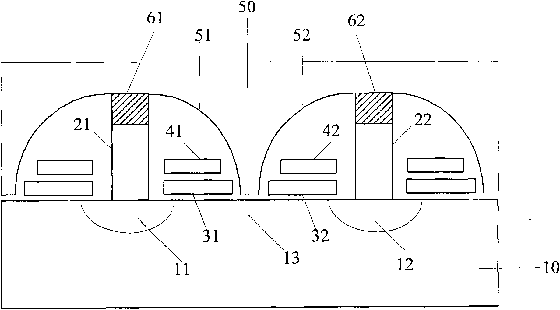
[0056] Please refer to figure 1 , figure 1 Shown is a schematic structural diagram of a non-contact silicon nitride split-gate flash memory sharing a word line according to a preferred embodiment of the present invention. The present invention proposes a non-contact silicon nitride split-gate flash memory sharing a word line, comprising: a semiconductor substrate 10 having source regions 11 and drain regions 12 arranged at inte...


PUM


Abstract

The invention provides a word line-sharing contactless silicon nitride split gate type flash memory and a manufacturing method thereof. In the obtained flash memory device, two storage bit cells share one word line, different operating voltages are applied to the word line, a first control gate, a second control gate, a first bit line and a second bit line to read, program and erase the storage bit cells, and the bit line-sharing structure enables the split gate type flash memory to effectively reduce the area of a chip under the condition of keeping the electric isolation performance of the chip unchanged and simultaneously can avoid the over-erase problems. Meanwhile, the contactless design enables the flash memory device to have the characteristics of small size and process compatibility with the CMOS traditional process, thereby being beneficial to further reducing the size of the device.

Description

technical field [0001] The invention relates to the field of semiconductor design and manufacture, and in particular to a word line-sharing non-contact silicon nitride split-gate flash memory and a manufacturing method thereof. Background technique [0002] Flash memory has become a research hotspot in non-volatile memory due to its convenience, high storage density, and good reliability. Since the first flash memory product came out in the 1980s, with the development of technology and the storage needs of various electronic products, flash memory has been widely used in mobile and communication devices such as mobile phones, notebooks, handheld computers and U disks. , flash memory is a kind of non-volatile memory. Its operating principle is to control the switch of the gate channel by changing the critical voltage of the transistor or memory cell to achieve the purpose of storing data, so that the data stored in the memory will not be lost due to power interruption. Disap...

Claims


Application Information

Patent Timeline
Patent Type & Authority Patents(China)
IPC IPC(8): H01L27/115H01L21/8247
Inventor 曹子贵
Owner SHANGHAI HUAHONG GRACE SEMICON MFG CORP
Why Eureka
Try Eureka