Liquid crystal display panel and manufacturing method thereof

A liquid crystal display panel and manufacturing method technology, applied in the direction of instruments, nonlinear optics, optics, etc., can solve problems such as increasing manufacturing costs, increasing manufacturing process steps, affecting product yield, etc., to reduce manufacturing costs and reduce manufacturing process steps , Improve the effect of product yield

Active Publication Date: 2010-10-27
SHANGHAI TIANMA MICRO ELECTRONICS CO LTD
View PDF0 Cites 15 Cited by
  • Summary
  • Abstract
  • Description
  • Claims
  • Application Information

AI Technical Summary

Problems solved by technology

[0007] However, the problem is that in the above-mentioned liquid crystal display panel, in order to realize the pre-tilt of the liquid crystal molecules after the voltage is applied, it is necessary to increase the process steps of manufacturing cracks or protrusions. The photolithography process is realized; in this way, at least one mask etching process is added in the manufacturing process of the liquid crystal display panel, and the manufacturing process steps are increased, which will affect the product yield and increase the manufacturing cost.

Method used


Image

  • Liquid crystal display panel and manufacturing method thereof
  • Liquid crystal display panel and manufacturing method thereof
  • Liquid crystal display panel and manufacturing method thereof

Examples


Embodiment 1

[0067] Figure 2A and Figure 2B It is a schematic structural diagram of the liquid crystal display panel in this embodiment. Only one pixel unit is shown in the figure, and a plurality of such pixel units are arranged in order in the liquid crystal display panel.

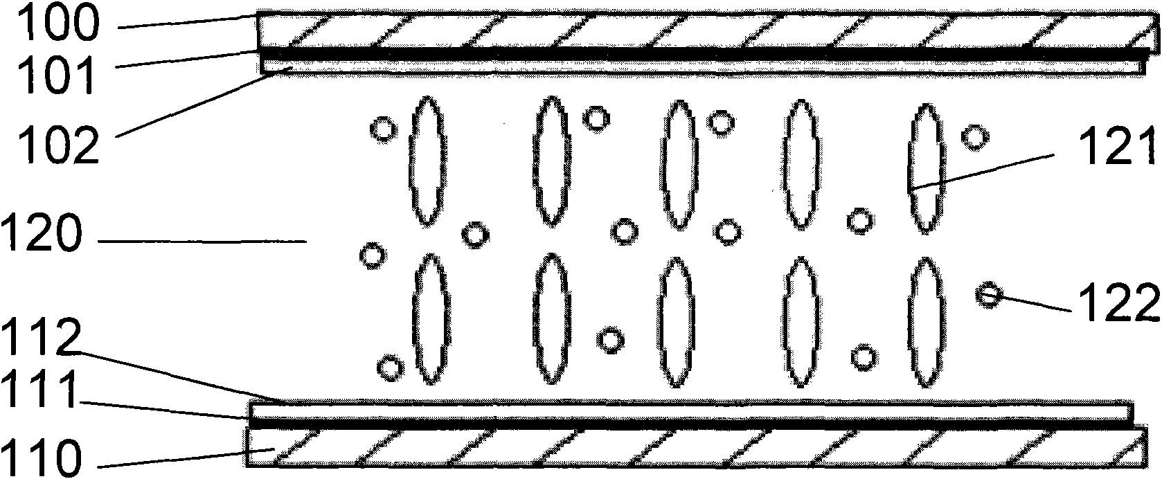
[0068] Such as Figure 2A As shown, the liquid crystal display panel includes: a first substrate 100 and a second substrate 110 disposed opposite to each other, and a liquid crystal layer 120 filled between the first substrate 100 and the second substrate 110 .

[0069] The first substrate 100 is, for example, a filter substrate, and the filter substrate 100 has an RGB color filter (not shown in the figure), a transparent electrode layer 101 and The alignment film 102 adjacent to the liquid crystal layer 120, wherein the transparent electrode layer 101 is a common electrode.

[0070] The second substrate 110 is, for example, an array substrate. The side of the array substrate 100 facing the liquid crystal layer...

Embodiment 2

[0078] Figure 3A , Figure 3B and Figure 3C It is a schematic structural diagram of the liquid crystal display panel in this embodiment.

[0079] Such as Figure 3A As shown, the liquid crystal display panel includes: a first substrate 200 and a second substrate 210 disposed opposite to each other, and a liquid crystal layer 220 filled between the first substrate 200 and the second substrate 210 .

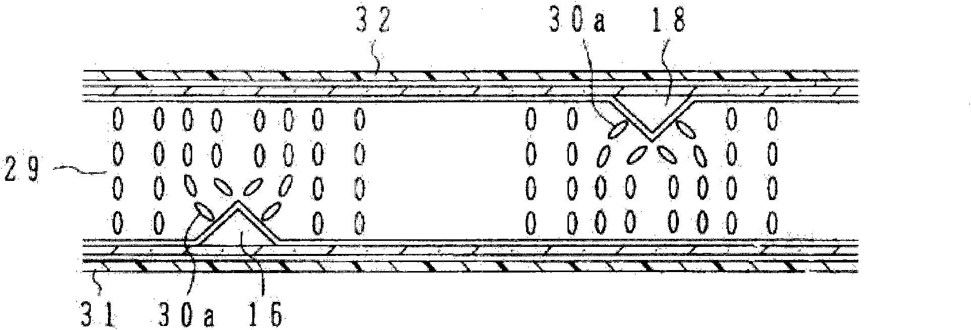
[0080] The first substrate 200 is, for example, a filter substrate, and the filter substrate 200 has RGB color filters (not shown in the figure), a transparent electrode layer 201 and an alignment film 202, wherein the transparent electrode layer 201 is the common electrode. The second substrate 210 is, for example, an array substrate. The array substrate 200 has a transparent electrode layer 211 and an alignment film 212, wherein the transparent electrode layer 211 is a pixel electrode; 200 and the anchor 222 of the negative liquid crystal molecule 221 pretilt angle on the ...

Embodiment 3

[0089] Figure 4 It is a schematic structural diagram of a liquid crystal display panel in this implementation.

[0090] As shown in the figure, the LCD panel includes:

[0091] The first substrate 300; the second substrate 310, arranged opposite to the first substrate 300; the liquid crystal layer 320, sandwiched between the first substrate 300 and the second substrate 310, the liquid crystal layer 320 contains a An anchor 322 for the pretilt angle of liquid crystal molecules 321 in the liquid crystal layer 320 on the surface of the first substrate 300 or the surface of the second substrate 310 ; the external electrode 305 is located on the side of the first substrate 300 facing away from the liquid crystal layer 320 . The composition and structure of the liquid crystal display panel are similar to those in the first embodiment, and will not be repeated one by one. In other embodiments of the present invention, the external electrodes may also be located on the side of the ...


PUM


Abstract

The invention provides a liquid crystal display panel and a manufacturing method thereof. The liquid crystal display panel comprises a first substrate, a second substrate which is opposite to the first substrate and a liquid crystal layer which is arranged between the first and the second substrates, wherein under the situation of non-electrification, liquid crystal molecules in the liquid crystal layer are arranged to be vertical to the first substrate, and the liquid crystal layer comprises an anchoring substance; the liquid crystal molecule which is close to the surface of the first substrate or the second substrate is pre-inclined under the situation of non-electrification through the anchoring substance. The liquid crystal display panel and the manufacturing method thereof are free from forming projection or crack and from changing other structures of a pixel unit, can realize the pre-inclination of the liquid crystal molecules, can simplify the manufacturing process procedure, can improve the yield of the product, and can reduce the cost.

Description

technical field [0001] The invention relates to the technical field of liquid crystal display, in particular to a liquid crystal display panel and a manufacturing method thereof. Background technique [0002] In recent years, large-sized, thin and light flat-panel displays have gradually taken center stage in the display market. According to the display principle, the flat panel display may include: a liquid crystal display (Liquid Crystal Display, LCD), a plasma display, an organic electroluminescent display, and the like. [0003] Among various display modes of liquid crystal displays, a vertical alignment (Vertical Alignment, VA) display mode is popular in the market due to its good viewing angle characteristics. In the LCD of the VA display mode, the long axis of the liquid crystal molecules in the pixel unit is perpendicular to the filter in the state of no power, and each pixel unit is divided into multiple domains (multi-domains). , the liquid crystal molecules in e...

Claims


Application Information

Patent Timeline
Patent Type & Authority Applications(China)
IPC IPC(8): G02F1/139G02F1/1337G02F1/1333
Inventor 吴勇马骏凌志华
Owner SHANGHAI TIANMA MICRO ELECTRONICS CO LTD
Why Eureka
Try Eureka