Wafer defect marking system
A technology for chip defects and wafers, which is applied in the direction of optical testing defects/defects, electrical components, semiconductor/solid-state device manufacturing, etc. It can solve problems such as difficulty in finding corresponding position marks, increased error rate, time-consuming and labor-consuming operations, etc.
- Summary
- Abstract
- Description
- Claims
- Application Information
AI Technical Summary
Problems solved by technology
Method used
Image

Examples
Embodiment Construction
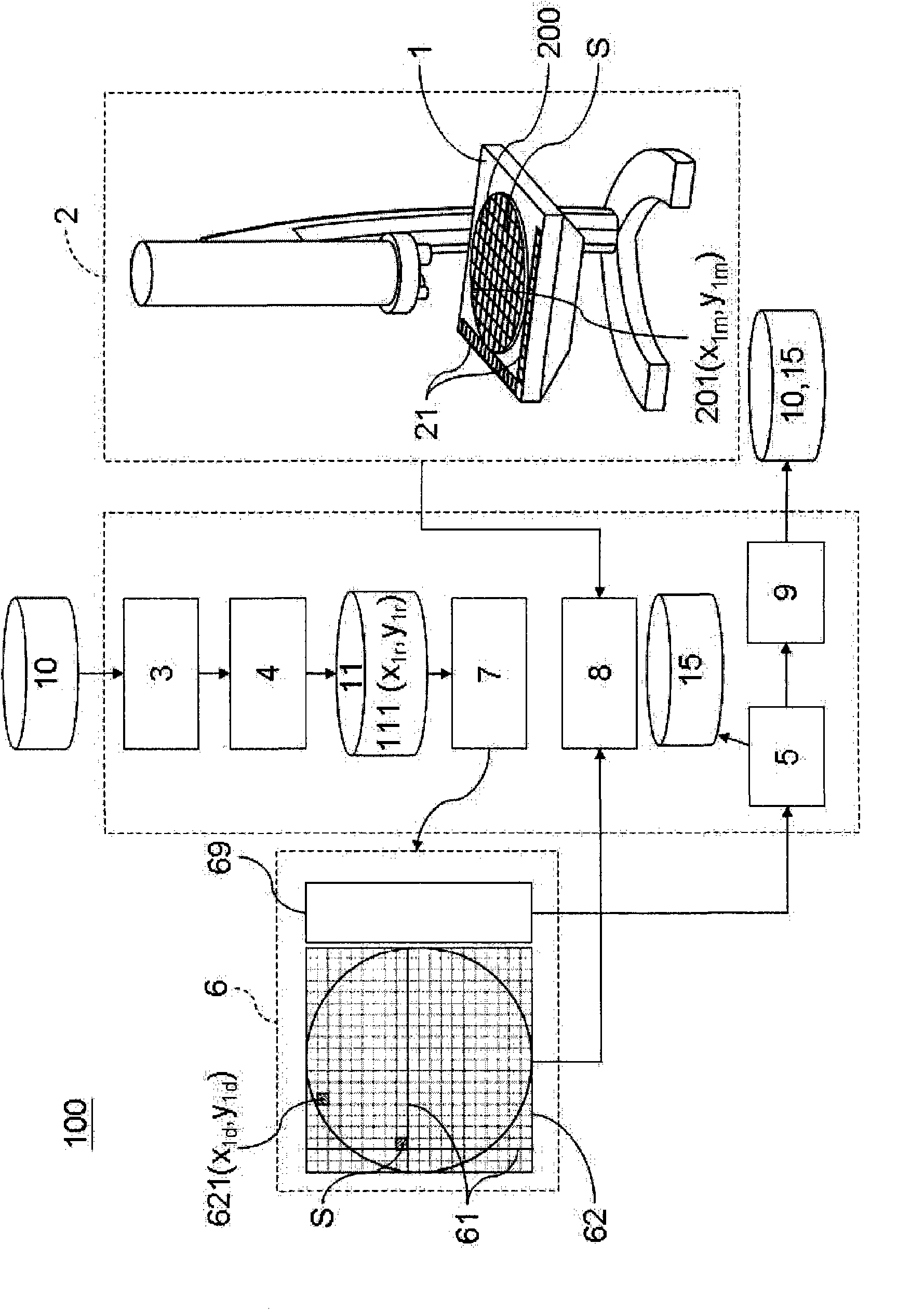
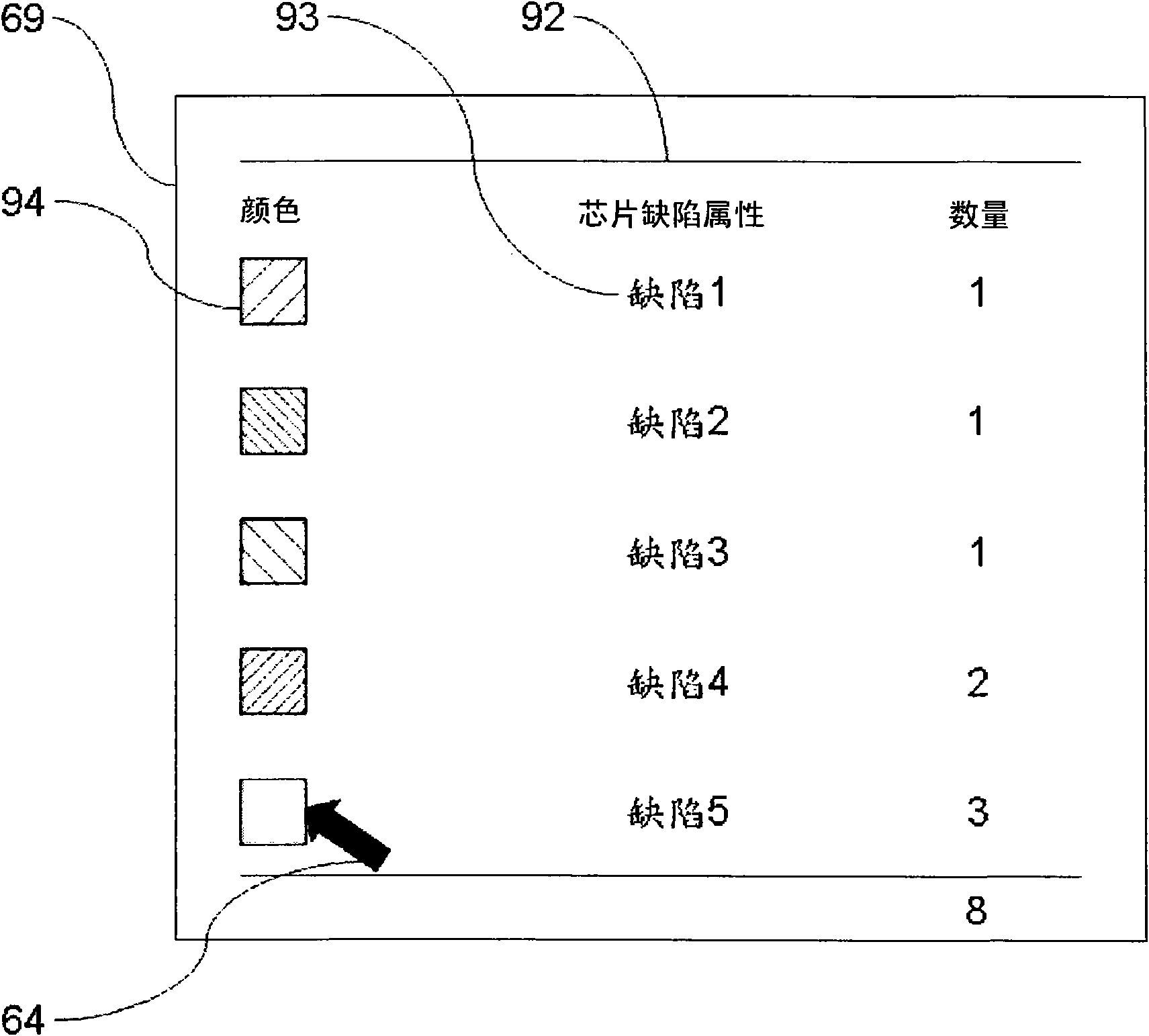
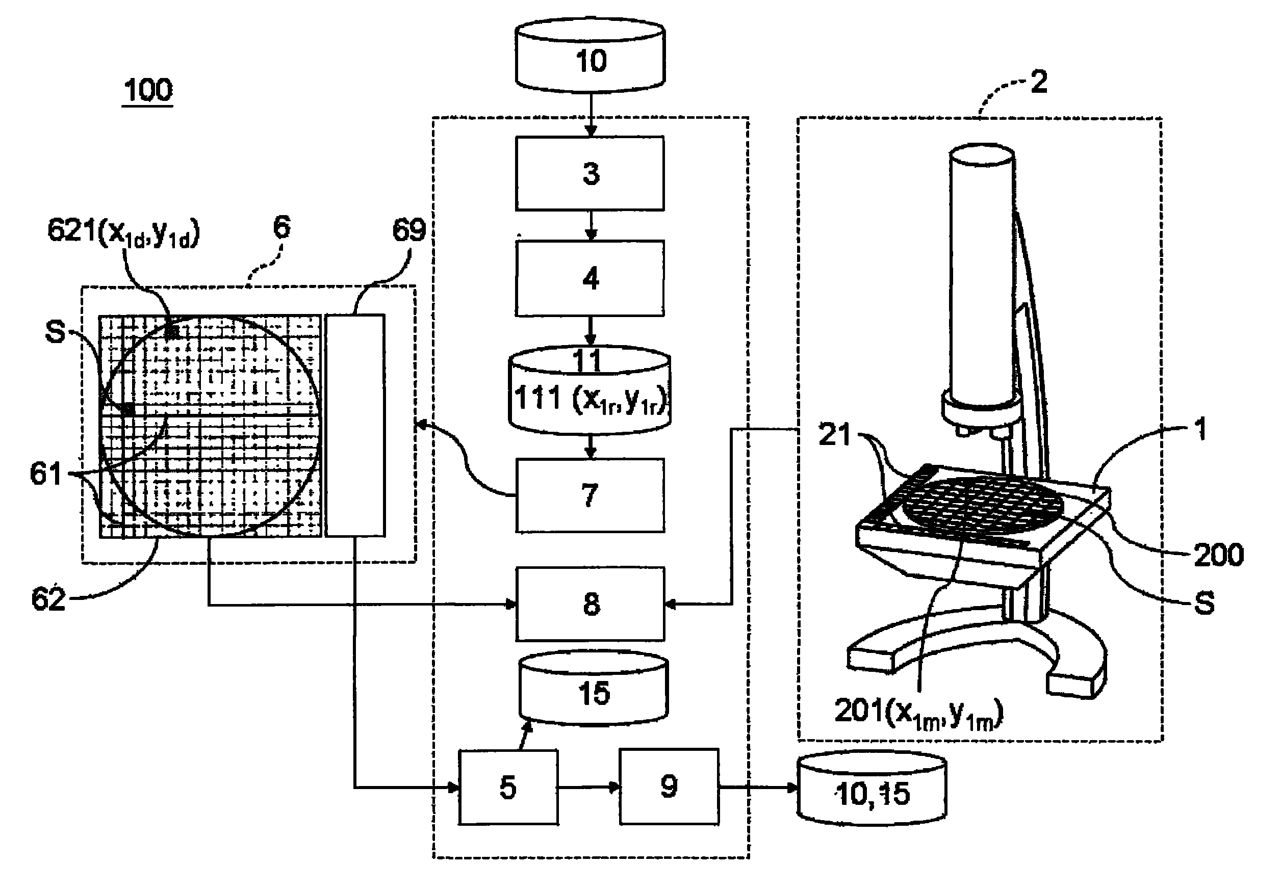
[0011] Since the present invention discloses a wafer defect marking system for wafer surface inspection, the basic principles and functions of wafer chip testing principles, image conversion and data transmission have been understood by those with ordinary knowledge in the relevant technical field, so the following The instructions in the text are no longer described in full. At the same time, the drawings compared below are schematic structural representations related to the features of the present invention, and are not and need not be completely drawn according to the actual size, so please describe first.
[0012] First please refer to figure 1 , the preferred embodiment of the present invention is shown in the figure, which is a wafer defect marking system 100, which is used to mark chips with defects on the wafer 200. This wafer defect marking system 100 includes a carrying platform 1, a microscopic observation module 2. The reading module 3 , the first computing module...
PUM
 Abstract
Description
Claims
Application Information
 - R&D
- Intellectual Property
- Life Sciences
- Materials
- Tech Scout
- Unparalleled Data Quality
- Higher Quality Content
- 60% Fewer Hallucinations
Browse by: Latest US Patents, China's latest patents, Technical Efficacy Thesaurus, Application Domain, Technology Topic, Popular Technical Reports.
© 2025 PatSnap. All rights reserved.Legal|Privacy policy|Modern Slavery Act Transparency Statement|Sitemap|About US| Contact US: help@patsnap.com