Liquid crystal display
A liquid crystal display device and liquid crystal layer technology, applied in liquid crystal materials, optics, instruments, etc., can solve problems such as image defects and singular points, and achieve the effect of high contrast characteristics
- Summary
- Abstract
- Description
- Claims
- Application Information
AI Technical Summary
Problems solved by technology
Method used
Image
Examples
Embodiment approach 1
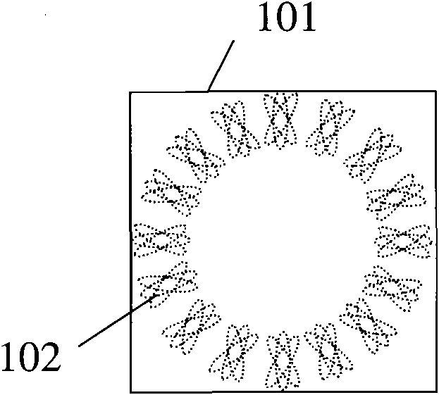
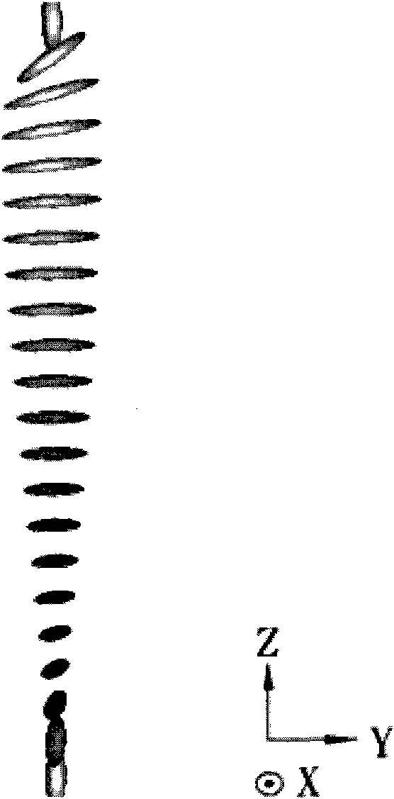
[0059] This embodiment is an alignment device using bumps or fringe electric fields under a non-rubbing alignment framework. Such as Figure 7 Shown is a structural diagram of twisted vertically aligned liquid crystals in a single pixel display area 701 using surrounding bumps 702 to achieve an alignment effect. exist Figure 7 In the schematic diagram of , no voltage is applied to the liquid crystal layer, and the twisted vertical alignment liquid crystal used is a negative nematic liquid crystal material, and an appropriate chiral agent is also mixed to make Δnd and d / p meet the optimal parameter conditions. The initial liquid crystal molecules are made perpendicular to the surface of the substrate by the vertical alignment film, and the liquid crystal molecules close to the bump structure will tilt toward a specific direction to form a pre-tilt angle. Figures 8A to 8D Under the conditions of Δnd=0.56 and d / p=0.278, the result of using 3D finite element analysis to simula...
Embodiment approach 2
[0065] This embodiment is also based on the framework of non-friction alignment, using the electrode pattern with periodic structure between the electrodes and the electrode gap as the first alignment device, and matching the surrounding bump structure, the surrounding concave structure or the surrounding electrode pattern structure The formed edge oblique electric field distribution is used to control the twisted vertically aligned liquid crystal molecules to arrange in a specific direction. Figure 12 Take the surrounding edge oblique electric field structure 1201 as an example, and the substrate electrode 1202 under the display area is configured as the first alignment device such as structures (1)-(7). In the above structure, the width of the etching gap L2 between the lower substrate alignment electrode L1 and the ITO electrode is 3-5 μm, which can provide a symmetrical arrangement of the liquid crystal molecules. At the same time, because the electrode has an etching gap...
Embodiment approach 3
[0068] The above-mentioned alignment devices all allow the liquid crystal molecules to form a continuous domain arrangement, and further extension can also allow the molecules to form a multi-domain arrangement. Such as Figure 14 Shown is a schematic diagram of an alignment structure that enables liquid crystal molecules to form multiple domain arrangements; wherein, structures (1), (2) and (3) are respectively on the upper substrate 1401 and the lower substrate 1402, with bump structures 1403 or electrode gaps The structures 1404 are arranged in a "く" shape, while the structures (4) and (5) are arranged in a cross shape with bump structures 1405 or electrode gaps 1406 and combined with radial electrode gap structures 1407 . All of the above structures allow the liquid crystal molecules to form an arrangement of multiple domains.
PUM
 Abstract
Description
Claims
Application Information


