

Glass ball cavity encapsulation method of light emitting diode
A technology of light-emitting diodes and packaging methods, which is applied in the direction of electrical components, circuits, semiconductor devices, etc., can solve the problems of poor light transmission of lenses, poor moisture resistance of organic matter, and poor light transmission performance, and achieve small viewing angles, not easy to age, and good Isophotic effect
- Summary
- Abstract
- Description
- Claims
- Application Information
AI Technical Summary
Benefits of technology
Problems solved by technology
Method used
Image

Examples
Embodiment 1
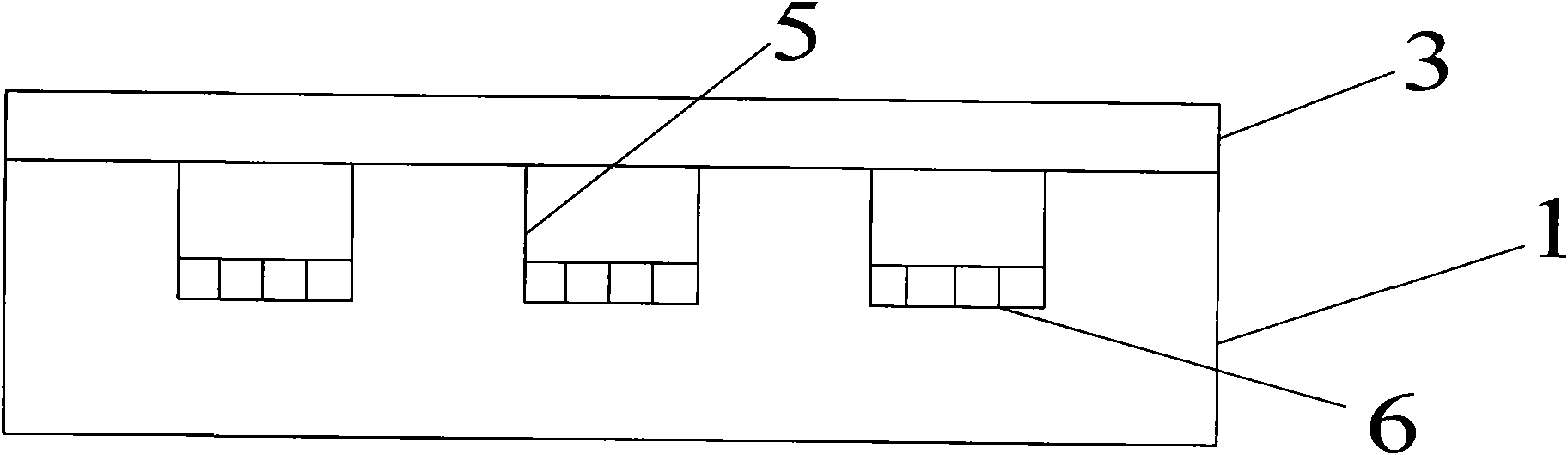
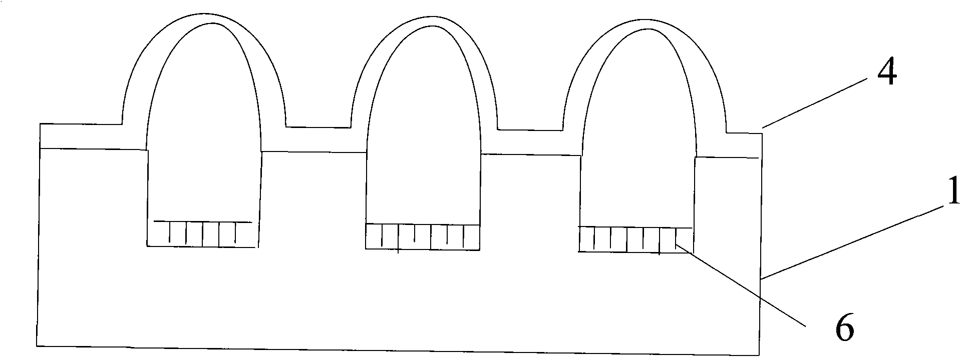
[0029] A method for encapsulating a light-emitting diode in a glass bulb cavity, comprising the following steps: the first step is to prepare a glass package with a microcavity on the back and a microlens on the front on a glass wafer; the glass package is prepared by positive pressure thermoforming , its size is slightly larger than the light-emitting diode (LED) chip of required packaging, and its height is greater than the thickness of the LED chip. The specific preparation method can be seen in embodiment 3-4. The second step, chip mounting: assemble the light-emitting diode (LED) chip On the silicon wafer substrate; the assembly process includes the lead-out of the LED chip, the silicon wafer is provided with leads, and the leads can also be guided to the back through silicon vias. The third step is the phosphor coating process: the phosphor (YAG: ce3+) Mix it with silica gel (Jiuqi brand WH-7 type silicone sealant produced by Nanjing Xilite Adhesive Co., Ltd.), and evenly...
Embodiment 2
[0031] Embodiment 2 A glass bulb cavity packaging method for light emitting diodes, comprising the following steps:
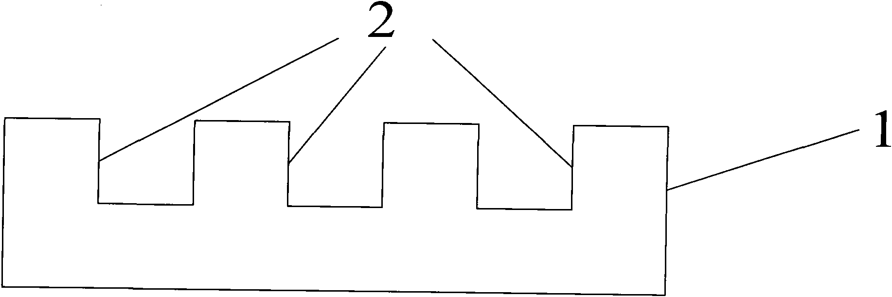
[0032] The first step is to prepare a glass lens array for sealing light-emitting diode (LED) chips on Pyrex7740 glass; under high temperature, the heat release agent releases gas, which forms a convex lens due to blowing out of the silicon microgroove when the glass is melted, and simultaneously under the lens A microcavity is formed, enabling a light emitting diode (LED) chip to be placed and sealed within the microcavity under the glass lens. For the preparation method of the glass lens microcavity, see the following embodiments of the present invention. The following examples of the present invention describe the method of making glass lenses by positive pressure forming. The glass microcavity prepared by the method described in the embodiment behind this embodiment adopts different microgroove aspect ratios, and the time and temperature of glass molding a...
Embodiment 3
[0037] Embodiment 3 A method for manufacturing a wafer-level glass lens microcavity, comprising the following steps:
[0038] In the first step, a specific pattern is formed on an Si wafer (such as a 4-inch wafer) by etching using a Si micromachining process, and the micromachining process of the pattern structure on the Si wafer is a wet etching process or a dry inductively coupled plasma One of the bulk (ICP) etching process, reactive ion etching or deep reactive ion etching, the pattern can be a square or circular groove array, or a number of different graphics, (in fact, three-dimensionally, Engraving a specific pattern is to carve a groove on a silicon wafer, which is a pattern in two dimensions), and the aspect ratio of the microgroove can be less than 1:1 or greater than 1:1, for example: 2:1, 3:1, 4:1 , 7:1, 10:1, 15:1, 20:1, 25:1, the glass microcavity with high aspect ratio will provide more rheological space for the glass, thus providing more space for the package c...
PUM
| Property | Measurement | Unit |
|---|---|---|
| Thickness | aaaaa | aaaaa |
| Thickness | aaaaa | aaaaa |
Abstract
Description
Claims
Application Information