
Memory device and methods for fabricating and operating the same

一种制造方法、操作方法的技术,应用在半导体/固态器件制造、电气元件、电固体器件等方向,能够解决程序化扰动、不便、影响等问题,达到增加储存密度、提高储存密度、增加位密度的效果

Active Publication Date: 2010-12-01
MACRONIX INT CO LTD
View PDF6 Cites 4 Cited by
  • Summary
  • Abstract
  • Description
  • Claims
  • Application Information

AI Technical Summary

Problems solved by technology

However, electrons are easily punched through between the two bottom junctions, which seriously causes leakage current in the memory structure.
Often programmatic perturbations due to close configuration of adjacent trenches
In addition, when adjacent vertical channel cells are too close to each other and not sufficiently isolated, the threshold voltage Vt of the target bit will be affected by the adjacent bit states
[0007] It can be seen that the above-mentioned existing memory element and the method for manufacturing and operating the memory element obviously still have inconvenience and defects in structure and use, and need to be further improved urgently.
In order to solve the above-mentioned problems, the relevant manufacturers have tried their best to find a solution, but for a long time no suitable design has been developed, and the general product has no suitable structure to solve the above-mentioned problems. This is obviously the relevant industry. Urgent problem

Method used


Image

  • Memory device and methods for fabricating and operating the same
  • Memory device and methods for fabricating and operating the same
  • Memory device and methods for fabricating and operating the same

Examples


Embodiment Construction

[0064] In order to further explain the technical means and functions adopted by the present invention to achieve the intended purpose of the invention, the specific implementation of the memory element and the method for manufacturing and operating the memory element according to the present invention will be described below in conjunction with the accompanying drawings and preferred embodiments. Mode, structure, feature and effect thereof are as follows in detail.

[0065] Examples of preferred embodiments of the present invention will be described in detail with reference to the accompanying drawings. Where possible, the same reference numbers and descriptions are used in the drawings to indicate the same or similar elements.

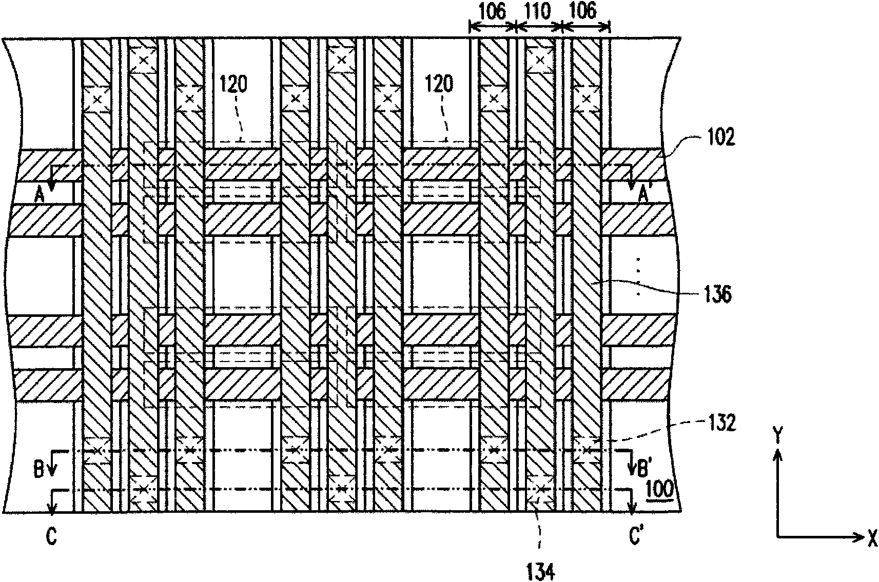
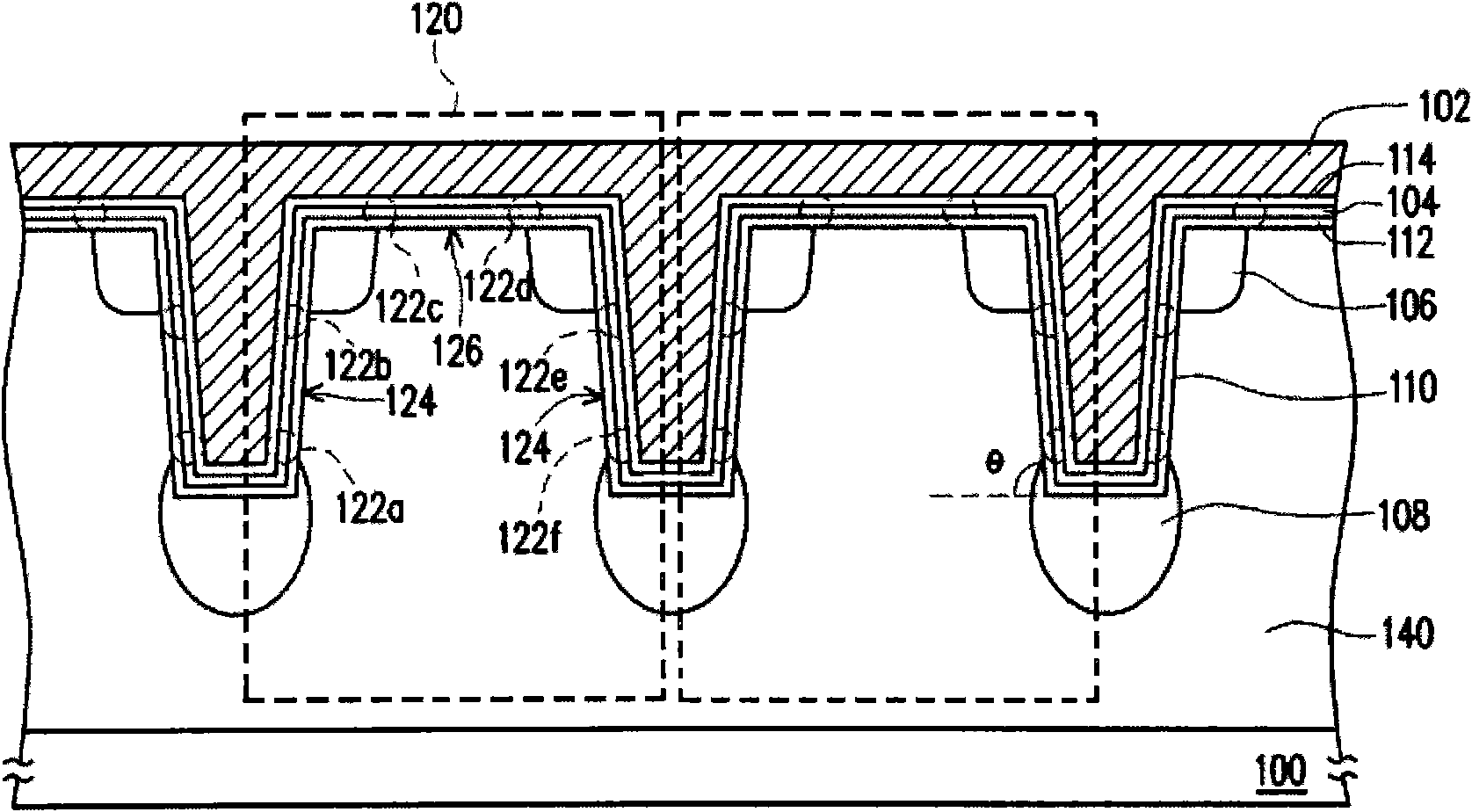
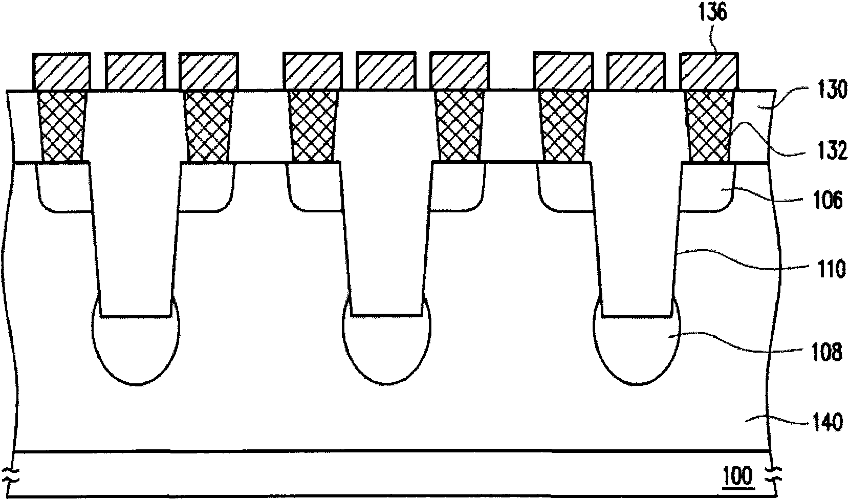
[0066] Figure 1A It is a schematic top view of a layout of a memory device according to an embodiment of the present invention, wherein an interlayer dielectric (ILD) is hidden. Figure 1B According to an embodiment of the present invention such as ...


PUM


Abstract

The invention relates to a memory device and method for fabricating and operating the same. The memory device is described, which includes a substrate, a conductive layer, a charge storage layer, a plurality of first doped regions and a plurality of second doped regions. The substrate has a plurality of trenches formed therein. The conductive layer is disposed on the substrate and fills the trenches. The charge storage layer is disposed between the substrate and the conductive layer. The first doped regions are configured in the substrate adjacent to both sides of an upper portion of each trench, respectively. The first doped regions between the neighbouring trenches are separated from each other. The second doped regions are configured in the substrate under bottoms of the trenches, respectively. The second doped regions and the first doped regions are separated from each other, such that each memory cell includes six physical bits. The the bit density is increased and the storage density is increased without effecting the layout size.

Description

technical field [0001] The present invention relates to a semiconductor element, in particular to a memory element, as well as a manufacturing method and an operation method of the memory element. Background technique [0002] Memory is a semiconductor device designed to store information or data. As the functions of computer microprocessors become more and more powerful, the programs and calculations performed by the software also increase. Therefore, the memory capacity requirements are getting higher and higher. Among all kinds of memory products, non-volatile memory allows multiple data programming, reading and erasing operations, and the data stored in it can be preserved even after the memory is powered off. Based on the above advantages, non-volatile memory has become a memory widely used in personal computers and electronic equipment. [0003] Electronically programmable and erasable non-volatile memory technologies based on charge storage structures are used in a...

Claims


Application Information

Patent Timeline
Patent Type & Authority Applications(China)
IPC IPC(8): H01L27/115H01L21/8247G11C16/10G11C16/14G11C16/26H10B69/00
CPCH01L27/11521G11C16/0475H01L27/11568H10B41/30H10B43/30
Inventor 杨怡箴吴冠纬陈柏舟张耀文卢道政
Owner MACRONIX INT CO LTD
Learn More