Pixel array structure

A pixel array and pixel technology, which is applied in the structural design of liquid crystal panels, can solve the problems of not being too close, loss of pixel aperture ratio, common voltage and gate line misconduction, etc., so as to avoid misconduction and reduce losses Effect

Inactive Publication Date: 2010-12-15
AU OPTRONICS CORP
View PDF0 Cites 0 Cited by
  • Summary
  • Abstract
  • Description
  • Claims
  • Application Information

AI Technical Summary

Problems solved by technology

However, since the positioning of the via hole must consider the line width and overlap of the photoresist coating process, exposure process, and development process, the specific position of the via hole will cause a serious loss to the pixel aperture ratio, thereby affecting the transmittance. and increased backlight loss
In addition, the distance between the via hole and the gate line of the pixel should not be too close, so as to avoid false conduction between the common voltage and the gate line.

Method used


Image

  • Pixel array structure
  • Pixel array structure

Examples


Embodiment Construction

[0019] Specific embodiments of the present invention will be described in detail below with reference to the accompanying drawings.

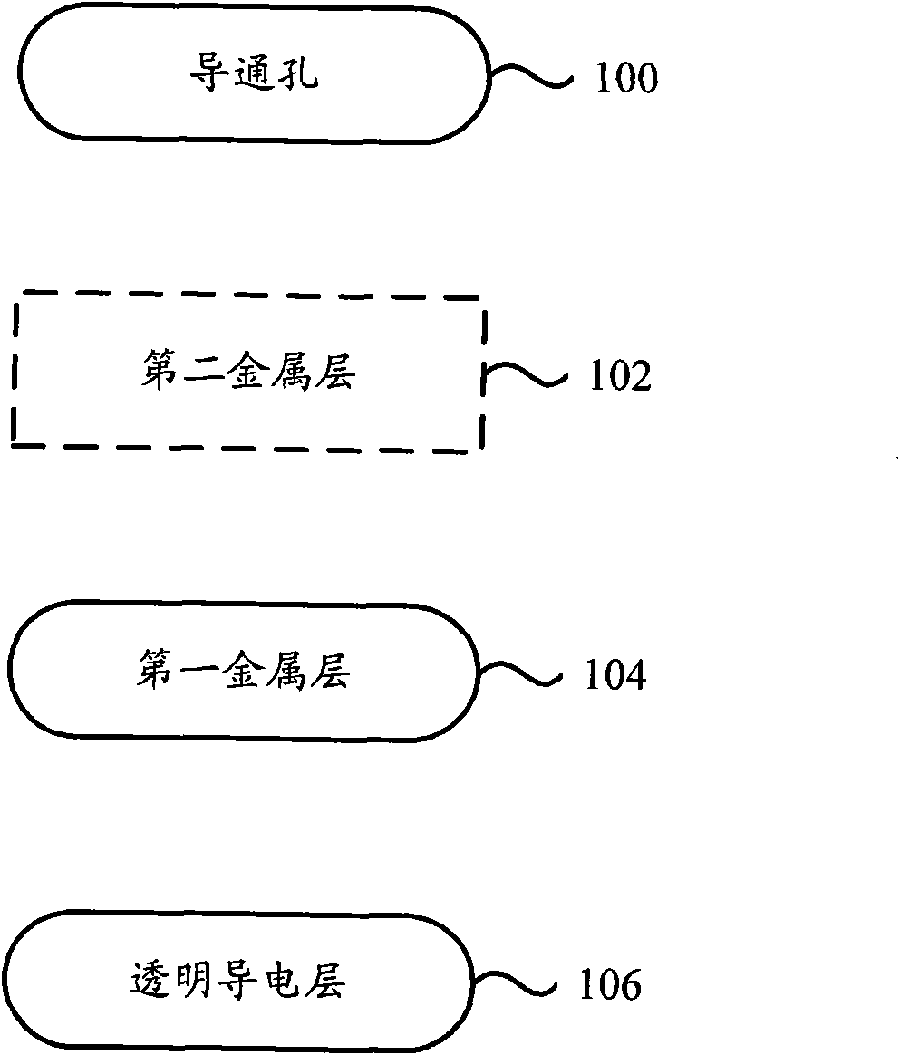
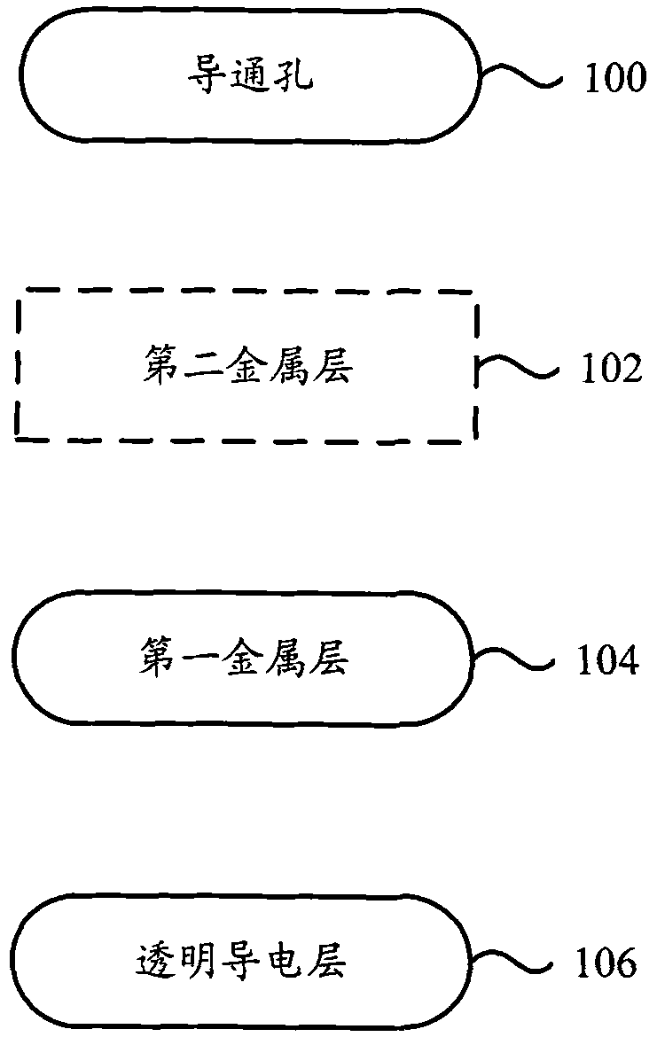
[0020] As mentioned above, in the existing mesh-com design of the pixel array structure, the same pixel common voltage is used between two adjacent pixels, and the electrical conduction is performed through the via hole, the metal layer and the ITO conductive layer in sequence. However, the specific location of the via hole may often cause a significant loss in pixel aperture ratio, because the distance between the via hole and the gate line of the pixel can neither be too large nor too small. Furthermore, if the distance between the two is too large, the aperture ratio of the pixel will be reduced, and if the distance is too small, false conduction between the via hole and the gate line will occur.

[0021] In order to solve this problem, the present invention provides a new pixel array structure. figure 1 According to a preferred embodiment o...


PUM


Abstract

The invention discloses a pixel array structure, which comprises a conductive hole, a first metal layer, a transparent conductive layer and a second metal layer, wherein the conductive hole is electrically connected to a common voltage of a pixel; the first metal layer is electrically connected to the common voltage of the pixel; the transparent conductive layer conducts the common voltage to another pixel next to the pixel, so that the common voltage is used as the common voltage of the another pixel; and the second metal layer is arranged between the first metal layer and the conductive hole to reduce the distance between the conductive hole and the gate line of the pixel, so that the opening ratio of the pixel is increased. When the pixel array structure is used, a virtual electrode is arranged between the metal layer and the conductive hole to reduce the distance between the conductive hole and the gate line of the pixel, so the loss caused by a netty common voltage structure to the opening ratio of the pixel is reduced. In addition, the virtual electrode can avoid micro-conduction of the conductive hole between the gate line and the common voltage when displacement or specification is changed.

Description

technical field [0001] The invention relates to the structural design of a liquid crystal panel, in particular to the design technology of the pixel array structure of the liquid crystal panel. Background technique [0002] In a conventional active matrix liquid crystal display, each pixel has a thin film transistor whose gate is connected to a horizontal scanning line, whose source is connected to a vertical data line, and whose drain is connected to a pixel electrode. For a pixel array structure containing many pixels, on the same scanning line in the horizontal direction, the gates of all thin film transistors are connected together, so the applied voltage is linked, for example, on a certain scanning line When a sufficiently large positive voltage is applied, all thin film transistors on this scanning line will be turned on, and the pixel electrodes on this scanning line will also be electrically connected to the data line in the vertical direction, and the corresponding...

Claims


Application Information

Patent Timeline
Patent Type & Authority Applications(China)
IPC IPC(8): G02F1/1362H01L27/02H01L23/528
Inventor 刘若梅
Owner AU OPTRONICS CORP
Why Eureka
Try Eureka