
Chip repairing method and chip stack structure

A chip stack and chip technology, which is applied in the field of chip repair methods and chip stack structures, can solve problems such as poor function and achieve the effect of reducing the number of chips.

Active Publication Date: 2010-12-22
IND TECH RES INST
View PDF1 Cites 8 Cited by
  • Summary
  • Abstract
  • Description
  • Claims
  • Application Information

AI Technical Summary

Problems solved by technology

It is a wasteful practice to throw away the entire chip just because a small part of the circuit is not functional, especially for high unit price integrated circuit products

Method used


Image

  • Chip repairing method and chip stack structure
  • Chip repairing method and chip stack structure
  • Chip repairing method and chip stack structure

Examples


Embodiment Construction

[0088]Exemplary embodiments are exemplified below and described in detail in conjunction with the accompanying drawings, so as to make the above-mentioned features and advantages more comprehensible.

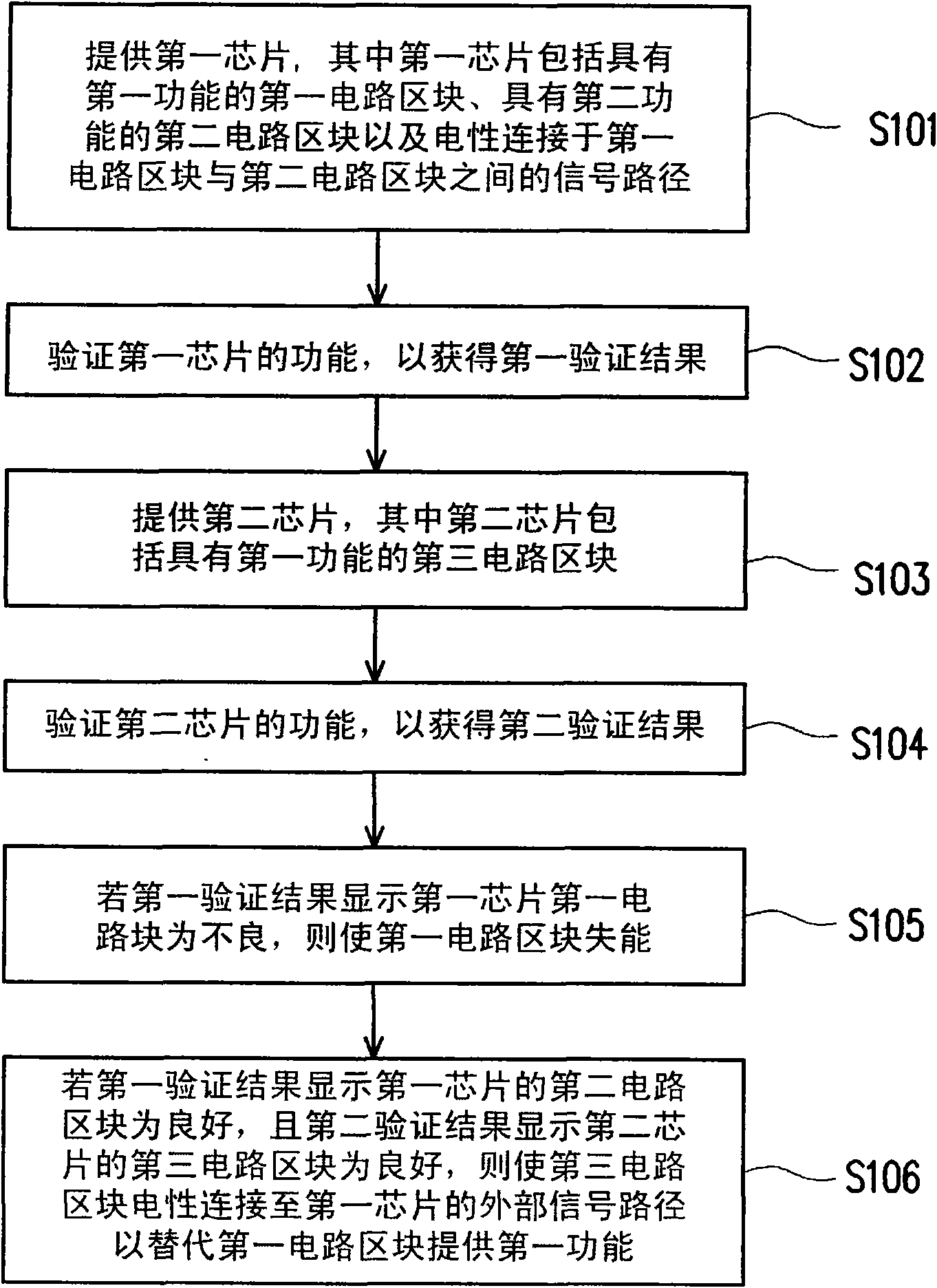
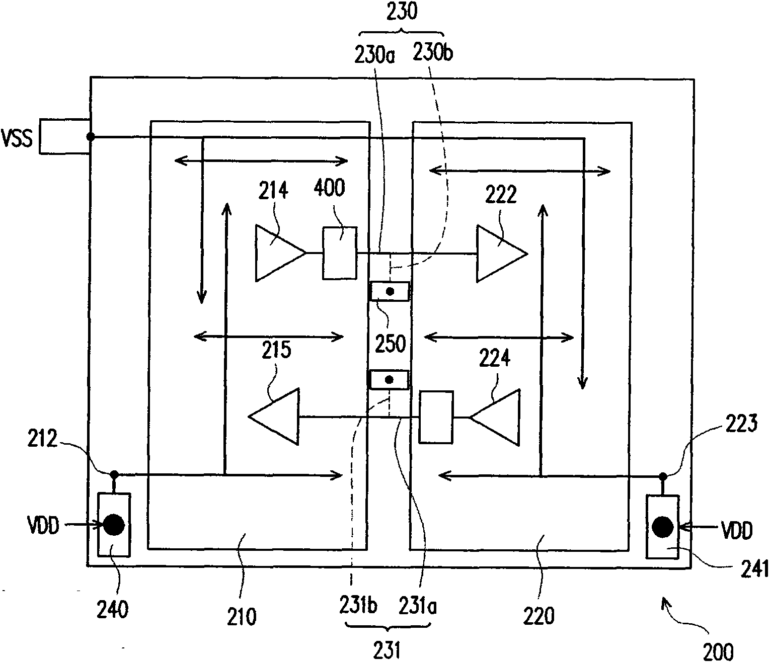
[0089] figure 1 It is a flowchart of a chip repairing method according to an embodiment of the present invention. figure 2 A schematic diagram of a first chip according to an embodiment of the present invention is drawn. The first chip 200 can be pre-divided into a plurality of circuit blocks, and each circuit block has an independent power terminal. In this embodiment, it is assumed that the first chip 200 is pre-divided into two circuit blocks, that is, the first circuit block 210 and the second circuit block 220 . In addition, the present embodiment assumes that the first circuit block 210 and the second circuit block 220 have independent first power supply terminals 212 and second power supply terminals 223 respectively, and the first circuit block 210 and the second circ...


PUM


Abstract

The invention discloses a chip repairing method applying chip stack structure, including that: a first chip and a second chip are provided, and the functions of the first chip and the second chip are verified, so as to obtain a first verification result and a second verification result. If the first verification result shows that a first circuit block of the first chip is defective, the first circuit block is disabled. If the first verification result shows that a second circuit block of the first chip is good and the second verification result shows that a third circuit block of the second chip is good, the third circuit block is electrically connected to a signal path, so as to substitute the first circuit block to provide first function. The invention can cause a plurality of defective chips to be combined into a good product, thus reducing the quantity of waste chips. Different signal and power transmission modes are formed by virtue of various through silicon vias in different collocation manners of a rigid line type switcher, and the invention can be used for transformation of signal and power transmission path without changing collocation manner of conductive bump and chip surface circuit.

Description

technical field [0001] The invention relates to a system chip repair, and in particular to a chip repair method and a chip stack structure. Background technique [0002] A spare (Spare) must be used for patching of an existing system on chip (SoC for short, also called a system-on-chip or system-on-chip). The so-called backup refers to duplicating a backup circuit block with the same function on the same chip. When it is known from the detection result of the system chip that the function of the original circuit block is invalid, the backup circuit block is activated to replace the original circuit block. Therefore, except for example, memory is regularly combined by many units with the same function and can be easily copied and shared, the backup of other arbitrary logic on the system chip often needs to pay an expensive price, and there is no backup result That is, when the original circuit block fails, the entire chip is completely useless and must be discarded. [000...

Claims


Application Information

Patent Timeline
IPC IPC(8): H01L21/50H01L21/60H01L25/18H01L23/52H01L21/66
CPCH01L2924/0002
Inventor 周永发蒯定明
Owner IND TECH RES INST
Learn More