Reactive ion etching method for etching silicon

A technology of reactive ion etching and reaction, which is applied in the field of reactive ion etching and etching of silicon, can solve the problems of reducing etching efficiency, process fluctuations, and efficiency reduction, etc., to prolong the access time and reduce the Effect of Small Undercut Effect and Bowl Effect

Active Publication Date: 2014-09-03
ADVANCED MICRO FAB EQUIP INC CHINA
View PDF3 Cites 0 Cited by
  • Summary
  • Abstract
  • Description
  • Claims
  • Application Information

AI Technical Summary

Problems solved by technology

However, the (1) method generally needs to close the reactive ion etching machine, and the plasma will be completely extinguished, and the etching of silicon holes usually requires multiple figure 1 The process shown is completed, so it is necessary to restart the machine and set parameters, which will greatly reduce the etching efficiency; in the second method, other gases are introduced, which is easy to cause fluctuations in the process, and a high vacuum pump is also required. The gas is pumped away, the etching efficiency is reduced, and it is difficult to maintain the stability of the radio frequency in the subsequent process

Method used


Image

  • Reactive ion etching method for etching silicon
  • Reactive ion etching method for etching silicon
  • Reactive ion etching method for etching silicon

Examples


Embodiment Construction

[0019] In order to make the object, technical solution and advantages of the present invention clearer, the present invention will be further described in detail below in conjunction with the accompanying drawings.

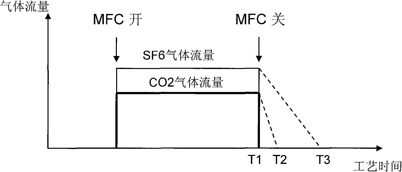
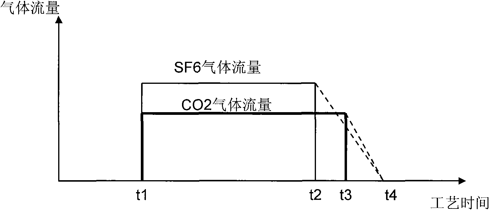
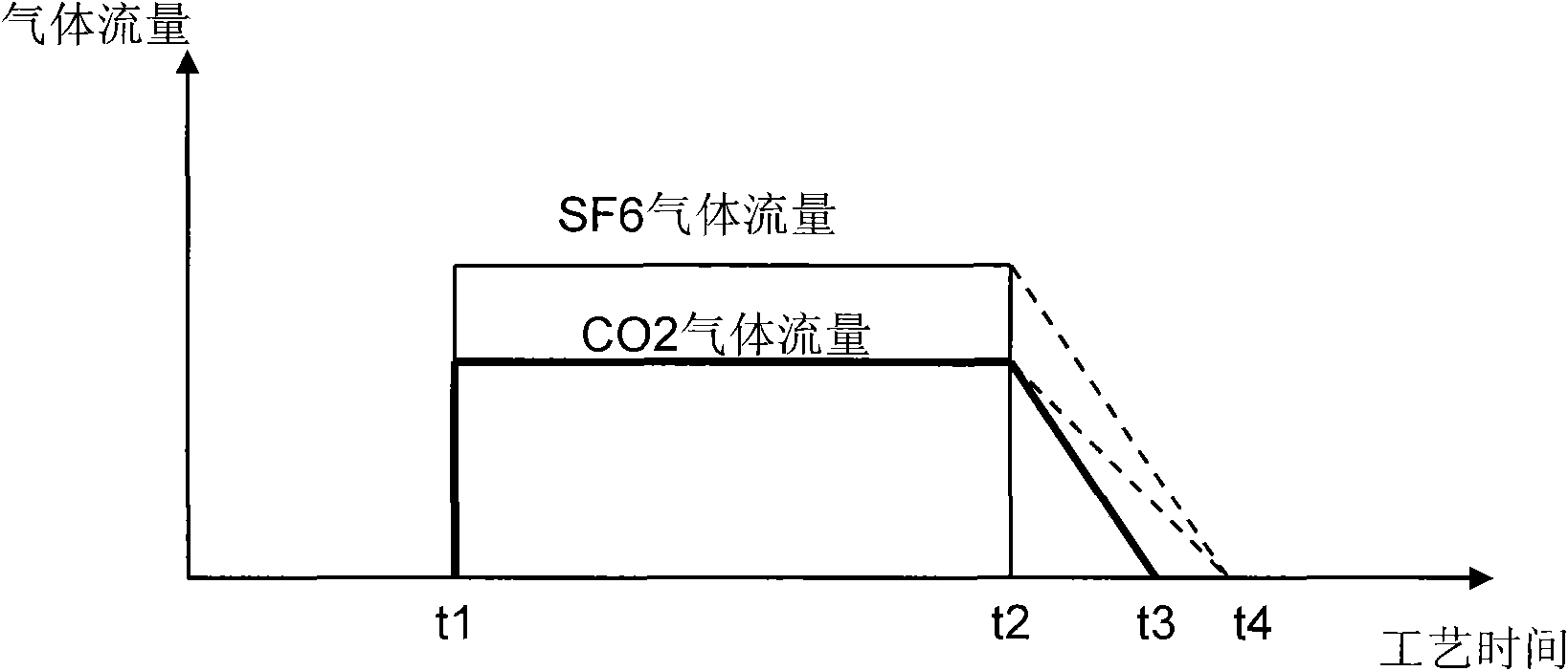
[0020] In this embodiment, taking the formation of TSV by reactive ion etching as an example, the depth of TSV reaches 50-200 μm, which is completed by the method of Steady-state deep silicon etch process. The reactive ion etching of this invention The method focuses on the control of the etching gas flow rate, therefore, other parameter settings of the reactive ion etching method, such as radio frequency (RF) power, air pressure, vacuum degree, etc., are not limited by the present invention. In this embodiment, during the etching process, the gas pressure ranges from 350 mTorr to 600 mTorr, the RF power is 1000 W, and the RF frequency is 60 MHz. In the steady-state deep silicon etching process, TSV etching is completed through multiple etching steps. In this embo...


PUM


Abstract

The invention provides a reactive ion etching method for etching silicon and belongs to the technical field of semiconductor manufacturing. In the reactive ion etching method, the adopted etching gas comprises a fluorine-containing gas and a gas which reacts with the silicon to form a passivation layer. When the etching process is finished, the fluorine-containing gas is stopped introducing first and then the gas which reacts with the silicon to form the passivation layer is stopped introducing. Holes formed by etching silicon in the method have smaller undercutting effect and bowl-shaped effect.

Description

technical field [0001] The invention belongs to semiconductor manufacturing technology, in particular to a reactive ion etching (Reactive Ion Etching, RIE) method, in particular to a reactive ion etching method for etching silicon. Background technique [0002] In the field of semiconductor manufacturing technology, it is often necessary to pattern and etch holes on silicon substrates or other silicon materials. In the prior art, dry RIE etching technology is usually used to generate F plasma ( Plasma) to etch silicon materials, for example, in the fields of MEMS ((Micro-Electro-Mechanical Systems, micro-electro-mechanical systems) and 3D packaging technology, it is usually necessary to perform bulk silicon etching to form deep through-silicon holes with a depth of several hundred microns (Through-Silicon-Via, TSV), the etching of deep silicon vias uses SF 6 and O 2 mixed gas for etching. [0003] In the process of reactive ion etching of silicon in the prior art, another...

Claims


Application Information

Patent Timeline
IPC IPC(8): C23F1/12
Inventor 崔在雄安东炫李柯奋吴万俊
Owner ADVANCED MICRO FAB EQUIP INC CHINA
Why Eureka
Try Eureka