Epitaxial growth method for improving inner quantum efficiency of GaN-based LED

A light-emitting diode, internal quantum efficiency technology, applied in gaseous chemical plating, coatings, electrical components, etc., can solve problems such as low internal quantum efficiency and brightness, influence of material crystal quality, and decline in radiation recombination efficiency, so as to improve luminescence. Efficiency and Brightness, Enhanced Quantum Localization Effect, Increased Effect of Internal Quantum Efficiency

Active Publication Date: 2013-03-20
YANGZHOU ZHONGKE SEMICON LIGHTING
View PDF0 Cites 0 Cited by
  • Summary
  • Abstract
  • Description
  • Claims
  • Application Information

AI Technical Summary

Problems solved by technology

Because there is usually a large lattice constant mismatch and thermal expansion coefficient difference between nitride and sapphire substrates, there are many crystal defects in the nitride epitaxial layer grown by metal organic chemical vapor deposition (MOCVD) epitaxy, such as Dislocations, etc., the crystal quality of the material is greatly affected
In particular, due to the polarization effect caused by stress caused by lattice mismatch, there is a large electric field in the quantum well, which leads to the separation of electron and hole wave functions in space, reduces the radiation recombination efficiency, and reduces the internal quantum efficiency and brightness of luminescence.

Method used


Image

  • Epitaxial growth method for improving inner quantum efficiency of GaN-based LED

Examples


Embodiment Construction

[0018] The epitaxial equipment used in this embodiment is a commercial machine produced by Germany AIXTRON company, and the model is Thomsaswan31x2'.

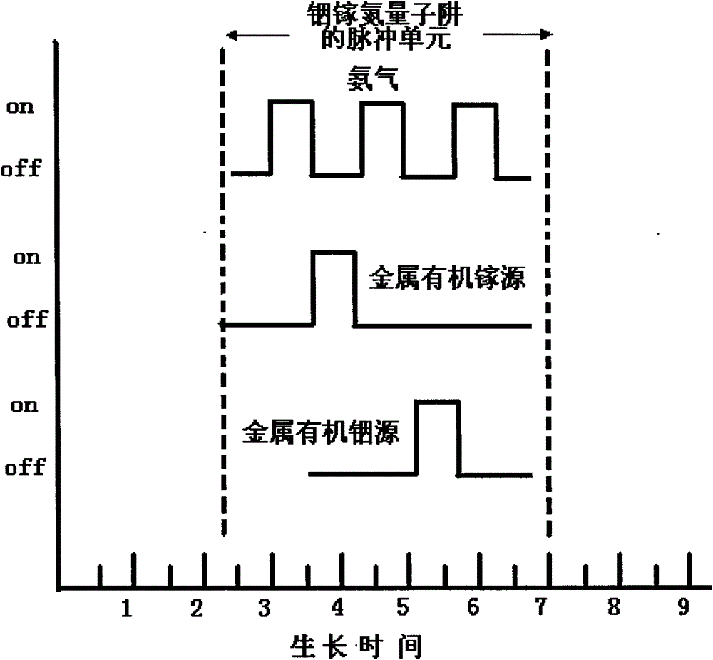
[0019] The V group source used was ammonia (NH 3 ), the Group III metal-organic source materials are trimethylgallium (TMGa) and trimethylindium (TMIn).

[0020] Carrier gas is N 2 or H 2 .

[0021] NH 3 , trimethylgallium (TMGa) and trimethylindium (TMIn) flow rates are 30 standard liters / minute (sl / m), 260 micromoles / minute (μmol / m) and 300 micromoles / minute (μmol / m) m).

[0022] The reaction chamber pressure is 300 Torr.

[0023] Steps:

[0024] After loading the 2-inch sapphire substrate into the MOCVD growth equipment, it is baked at high temperature in sequence to grow a low-temperature gallium nitride buffer layer, a gallium nitride nucleation layer, and an n-type gallium nitride layer.

[0025] Then grow the InGaN / GaN light-emitting active region. First, the temperature of the sapphire substrate was lowered to ...


PUM

PropertyMeasurementUnit
thicknessaaaaaaaaaa
thicknessaaaaaaaaaa

Abstract

The invention relates to an epitaxial growth method for improving the inner quantum efficiency of a GaN-based LED, belonging to the technical field of semiconductors. The method comprises the following steps of: alternately inputting ammonia gas as well as Group III metal organic source materials of gallium and indium in a growth reaction chamber in a pulsing way during the growth of an In-Ga-N quantum well layer of a GaN-based blue / green light LED active area; and forming a In-Ga-N quantum well luminous layer with high luminous efficiency in a modulation growth process under a set duration, a set interval and a set pulse period. The method can weaken an internally-built electric field of the In-Ga-N / GaN quantum well, improve the quantum localization effect, enhance the radiative recombination rate and increase the inner quantum efficiency of luminescence so as to improve the luminous efficiency and the brightness of the LED. The method is suitable for the MOCVD (Metallo Organic Chemical Vapor Deposition) epitaxial growth of a nitride-based blue / green light LED epitaxial material with high brightness and high luminous efficiency.

Description

technical field [0001] The invention belongs to the technical field of semiconductors, in particular to an epitaxial growth method for improving the internal quantum efficiency of gallium nitride-based blue light / green light emitting diodes. Background technique [0002] Gallium Nitride (GaN) is the third generation direct energy gap wide bandgap semiconductor with a bandgap width of 3.39eV. GaN-based green and blue light-emitting diodes (LEDs) have the advantages of high brightness, low energy consumption, long life, and fast response, and are widely used in full-color display, signal indication, and landscape lighting. In particular, the research and development of white LEDs made of GaN-based blue LEDs mixed with phosphors is progressing rapidly. The emission wavelength of white LEDs is only in the visible light region, which avoids the strong infrared radiation of incandescent lamps and can save a lot of energy. At the same time, white LEDs are small in size, long in li...

Claims


Application Information

Patent Timeline
Patent Type & Authority Patents(China)
IPC IPC(8): H01L33/12C23C16/44
Inventor 闫发旺宋雪云
Owner YANGZHOU ZHONGKE SEMICON LIGHTING
Why Eureka
Try Eureka