
MOS (Metal Oxide Semiconductor) grid base electrode switching tetrode

A tetrode and base technology, applied in the direction of electrical components, electric solid devices, circuits, etc.

Inactive Publication Date: 2013-05-01
王立模
View PDF4 Cites 0 Cited by
  • Summary
  • Abstract
  • Description
  • Claims
  • Application Information

AI Technical Summary

Problems solved by technology

Secondly, due to the complexity of the device structure and process, it is difficult to optimize the adjustment of the device's structural parameters and process parameters. For example, in order to ensure that the p+ penetration deep diffusion can exceed n+The doping concentration of the buried layer, the doping concentration of the n+ buried layer (the emitter region of the NPN tube) should not be too high, which makes it difficult to improve the current gain and current output capability of the NPN tube
Third, ESBT is a direct switch emitter current IE, no amplification function

Method used


Image

  • MOS (Metal Oxide Semiconductor) grid base electrode switching tetrode
  • MOS (Metal Oxide Semiconductor) grid base electrode switching tetrode
  • MOS (Metal Oxide Semiconductor) grid base electrode switching tetrode

Examples


Embodiment Construction

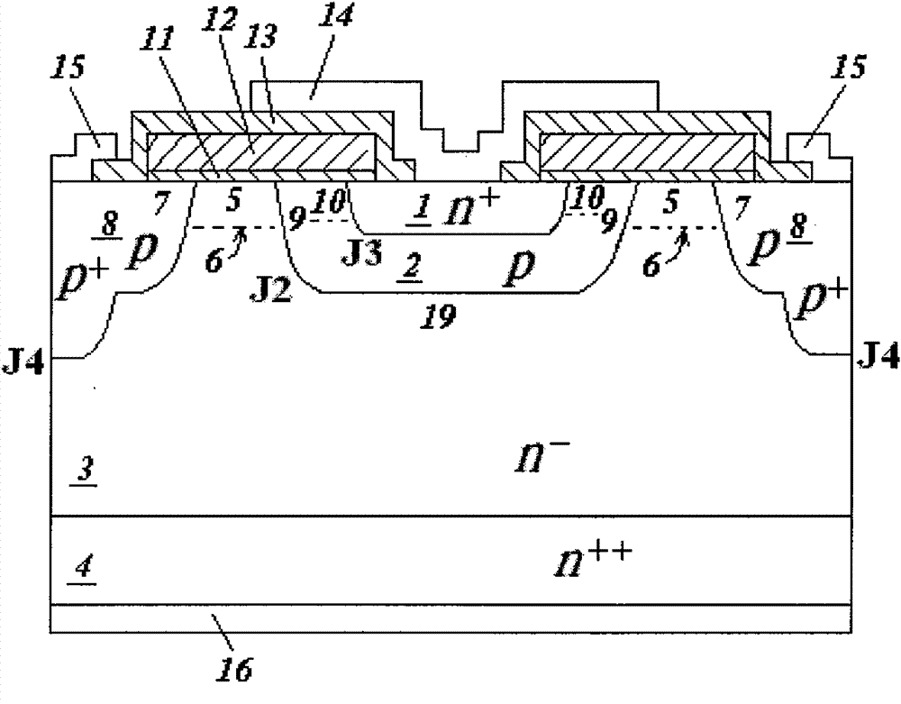
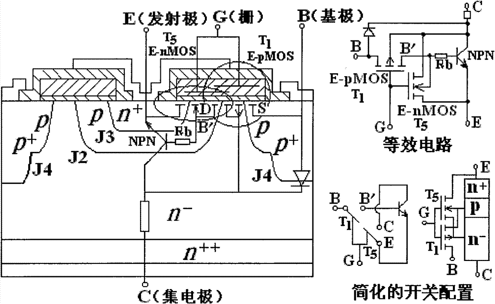
[0063] figure 2 Shown is an embodiment of a single-channel MOS gate-base switching quadrupole transistor of an enhanced p-channel MOS gate-base switching quadrupole transistor (E-pBSTT) with a planar gate structure, which uses a p-channel MOS gate switch A quadrupole transistor with base current of NPN tube. image 3 Shows its equivalent circuit and switch configuration. Its specific implementation is as follows. in n + n - Epitaxial layer 3 in the drift region. After the thick field oxidation is completed, the floating field limiting ring of the high voltage terminal ( figure 2 (not shown) high-concentration p+ doping in the independent prosthetic base region 8 while completing the high-concentration p+ doping. After the photolithography of the active area is completed, gate oxidation and doped polysilicon deposition are performed, and gate polysilicon 12 and gate oxide layer 11 are etched back. Using the gate polysilicon 12 and the gate oxide layer 11 as a mask, the...


PUM


Abstract

The invention relates to an MOS grid base electrode switching tetrode which is a novel four-terminal MOS grid power switching element which is additionally provided with an MOS control grid on the base electrode channel of a bipolar device (a bipolar transistor or a bipolar transistor in a bipolar transistor). The tetrode combines the advantages of the simplicity of an MOS grid driving circuit and the high current density conduction capacity of the bipolar device and has an amplification switching function. The invention provides the device structures and the specific implementation modes of a single channel and complementary channel MOS grid base electrode switching tetrode transistor with a plane grid and groove grid structure and an MOS grid base electrode switching tetrode transistor;the device structures and the specific implementation modes are compatible with the manufacturing processes of power MOSFET (Metal-Oxide-Semiconductor Field Effect Transistor) and IGBT (Insulated Gate Bipolar Translator) and are simpler much more than the structure and the process of a four-terminal emitter switching bipolar transistor (ESBT). The lambda negative resistance-type negative slope saturation characteristics of the transistors have better anti-dV / dt capacity, and the current negative temperature coefficient thereof are beneficial to the parallel connection of a large number of unit cells. The principles of the devices can also be used for manufacturing various compound semiconductor MOS grid base electrode switching tetrode transistors and thyristors.

Description

technical field [0001] The invention belongs to the field of semiconductor power switching devices, and in particular relates to a four-terminal power switching device using an insulating gate to control large current. [0002] The present invention includes the following closely related sub-inventions under the general idea of ​​using MOS gates to switch the small base currents of power bipolar devices to achieve switching their large output currents: single-channel MOS gate-base switching quadrupole transistors; complementary Trench MOS gate base switch quadrupole transistor; single channel MOS gate base switch quadrupole thyristor; complementary channel MOS gate base switch quadrupole thyristor. Background technique [0003] Power Metal-Oxide-Semiconductor Field Effect Transistor (Power MOSFET), Insulated Gate Bipolar Transistor (Insulated Gate Bipolar Transistor, referred to as IGBT), MOS Gate Thyristor (MOS-Gated Thyristor, referred to as MGT), etc. use MOS gate to cont...

Claims


Application Information

Patent Timeline
Patent Type & Authority Patents(China)
IPC IPC(8): H01L27/04H01L21/77
Inventor 不公告发明人
Owner 王立模
Features
  • Generate Ideas
  • Intellectual Property
  • Life Sciences
  • Materials
  • Tech Scout
  • Unparalleled Data Quality
  • Higher Quality Content
  • 60% Fewer Hallucinations
Learn More