Power supply compensation method and power supply compensation circuit

A technology of power supply compensation and adding circuit, which is applied in the direction of adjusting electrical variables, control/regulation systems, instruments, etc., can solve problems such as large wiring impedance, abnormal operation of near-end loads, and inability to compensate remote load voltage drops, etc., to overcome The Effect of Single-Ended Feedback

Inactive Publication Date: 2011-02-23
重庆节节高科技发展有限公司
View PDF4 Cites 24 Cited by
  • Summary
  • Abstract
  • Description
  • Claims
  • Application Information

AI Technical Summary

Problems solved by technology

Although this method can ensure that the remote load obtains the required normal working voltage, when the remote load current is large, the temperature is high, and the wiring impedance is large, in order to compensate for the voltage drop, the adjusted output voltage of the voltage source may be will be higher, which may cause the voltage obtained by the near-end load to be higher than the upper limit of its operating voltage, resulting in abnormal operation of the near-end load
[0005] It can be seen that although the voltage feedback compensation method in the prior art can compensate the voltage drop loss of a part of the load, it has the disadvantage of single-ended feedback, that is, the near-end voltage feedback method cannot compensate the remote load due to impedances such as PCB traces and filter inductors. However, the far-end voltage feedback method may cause the near-end load to obtain a voltage drop higher than the upper limit of its operating voltage due to the excessive feedback voltage drop, so that it cannot really satisfy all loads under the same voltage source. The voltage of the chip is within the requirements of its voltage operating range

Method used


Image

  • Power supply compensation method and power supply compensation circuit
  • Power supply compensation method and power supply compensation circuit
  • Power supply compensation method and power supply compensation circuit

Examples


Embodiment Construction

[0023] In order to make the purpose, technical solutions and advantages of the present invention clearer, the technical solutions in the embodiments of the present invention will be clearly and completely described below in conjunction with the accompanying drawings in the embodiments of the present invention. Obviously, the described embodiments are the Some, but not all, embodiments are invented. Based on the embodiments of the present invention, all other embodiments obtained by persons of ordinary skill in the art without making creative efforts belong to the protection scope of the present invention.

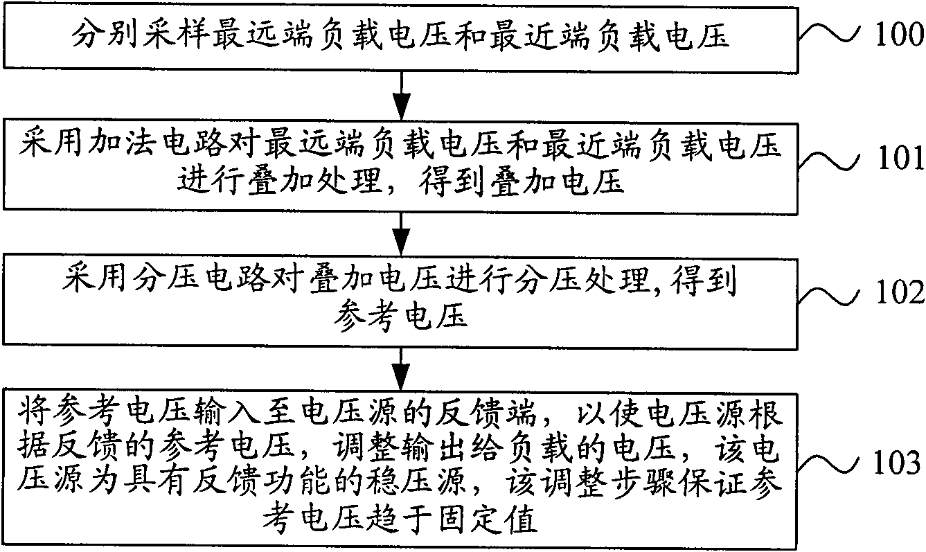
[0024] figure 1 It is a flow chart of Embodiment 1 of the power supply compensation method of the present invention, such as figure 1 As shown, this embodiment specifically includes the following steps:

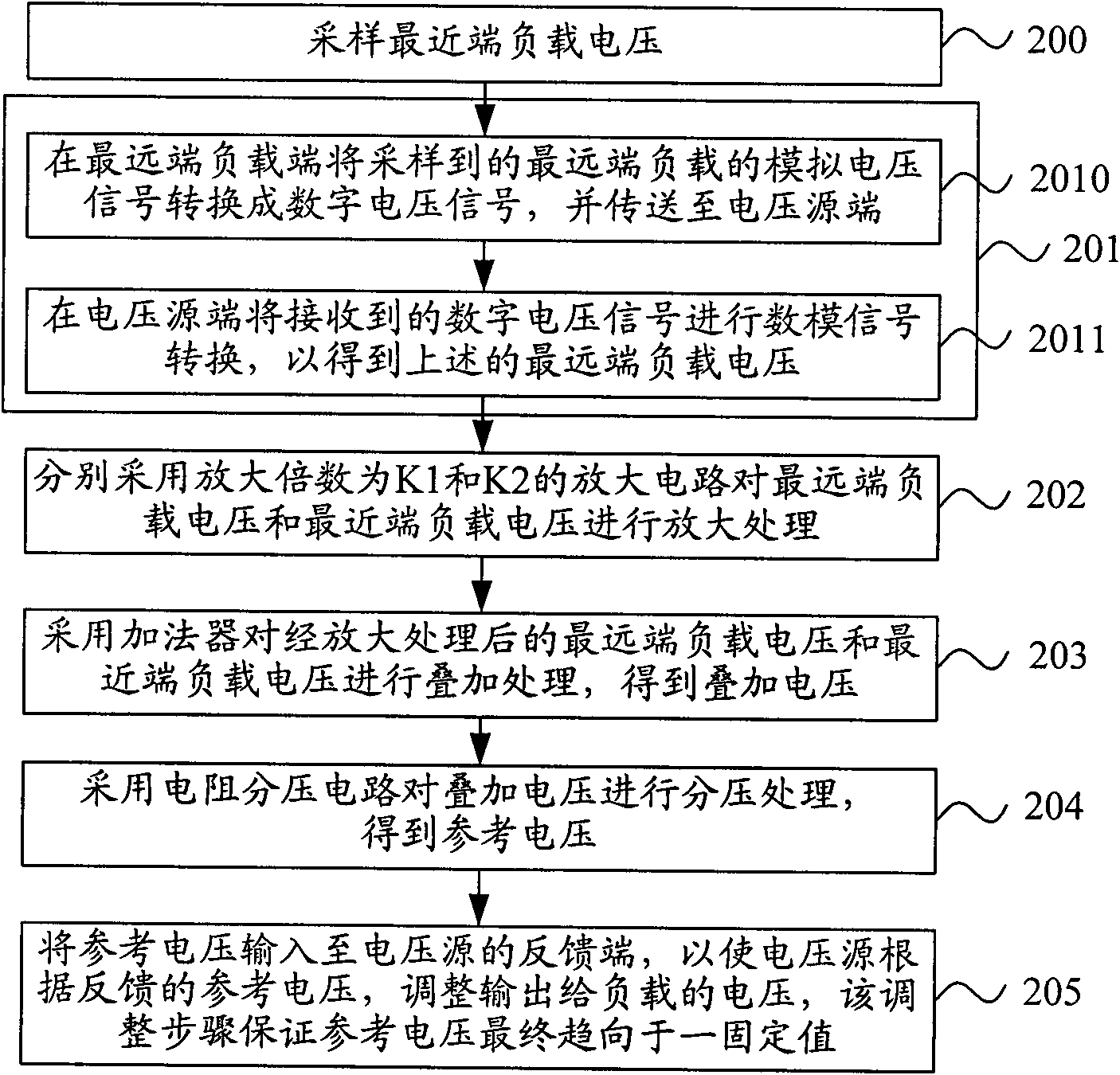
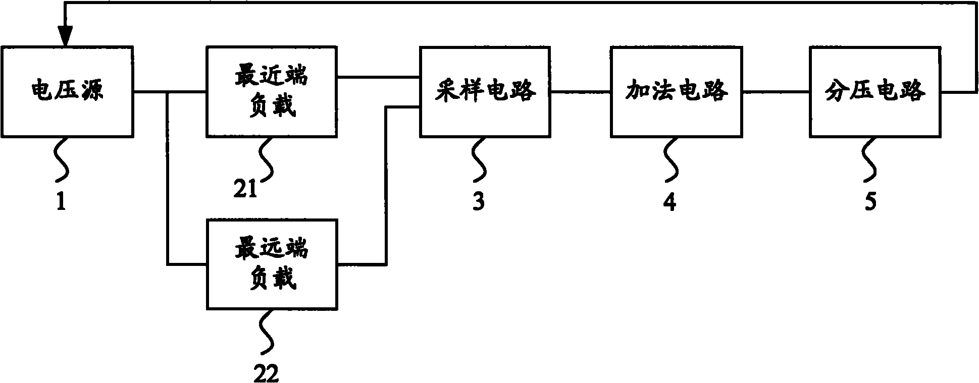
[0025] Step 100, respectively sampling the farthest end load voltage and the nearest end load voltage;

[0026] The power supply compensation method of the present inve...


PUM


Abstract

The invention provides a power supply compensation method and a power supply compensation circuit. The method comprises the following steps of: sampling farthest end load voltage and nearest end load voltage respectively; superposing the farthest end load voltage and the nearest end load voltage by using an adding circuit to obtain superposed voltage; dividing the superposed voltage by using a voltage dividing circuit to obtain reference voltage; and inputting the reference voltage into the feedback end of a voltage source, so that the voltage source adjusts the voltage which is output to a load according to the reference voltage which is fed back, wherein the voltage source is a stabilized voltage source with feedback function; and the adjusting step ensures that the reference voltage is close to a fixed value. Variable voltage drop between a far end load and a power supply is uniformly distributed to near end load voltage and far end load voltage, and the working voltage deviation of all load chips under an adjusted voltage source is ensured to be in a fixed range, so that the defect of single end feedback in the conventional power supply compensation method is effectively overcome.

Description

technical field [0001] The invention relates to the technical field of electronic communication, in particular to a power compensation method and a power compensation circuit. Background technique [0002] With the development of network communication technology, the current circuit board area is getting larger and larger, and the printed circuit board (PCB) traces are becoming thinner and thinner. The trace impedance introduced by this has become a non-negligible factor. Secondly, in order to achieve isolation and filtering, magnetic beads or inductors are usually connected in series at the end of the voltage source signal. The magnetic beads and inductors themselves also have a certain impedance. Therefore, factors such as PCB traces, inductors, and magnetic beads cause the There is a certain voltage drop loss between the terminal and the load. On the other hand, for the load, the load chip is usually set with an upper voltage limit and a lower voltage limit. If the volt...

Claims


Application Information

Patent Timeline
Patent Type & Authority Applications(China)
IPC IPC(8): G05F1/56
Inventor 肖群张寿棋
Owner 重庆节节高科技发展有限公司
Why Eureka
Try Eureka