Luminescent device formed by inverted luminous cell array and manufacture method thereof

A technology for light-emitting units and light-emitting devices, which is applied to electrical components, electrical solid-state devices, semiconductor devices, etc., can solve the problems of low production yield and complex process, and achieve the effect of improving production yield, simple process, and eliminating process difficulties.

Inactive Publication Date: 2011-03-02
APT ELECTRONICS
View PDF4 Cites 15 Cited by
  • Summary
  • Abstract
  • Description
  • Claims
  • Application Information

AI Technical Summary

Problems solved by technology

However, both of the above two processes require wiring in the grooves on the LED chip, the process is complex, and the production yield is low

Method used


Image

  • Luminescent device formed by inverted luminous cell array and manufacture method thereof
  • Luminescent device formed by inverted luminous cell array and manufacture method thereof
  • Luminescent device formed by inverted luminous cell array and manufacture method thereof

Examples


Embodiment 1

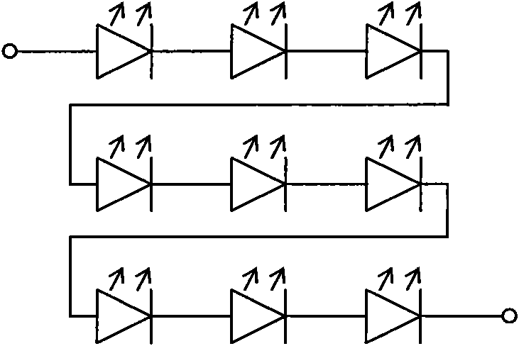
[0033] Please also see Figure 3 to Figure 7 ,in, image 3 is a schematic circuit diagram of Embodiment 1 of the light-emitting device of the present invention; Figure 4 It is a top view of the surface structure of Embodiment 1 of the light-emitting device of the present invention; Figure 5 yes Figure 4 A cross-sectional view of the light emitting device shown; Figure 6 yes Figure 4 The bottom view of the surface structure of the LED chip shown; Figure 7 yes Figure 4 Top view of the surface structure of the substrate shown.

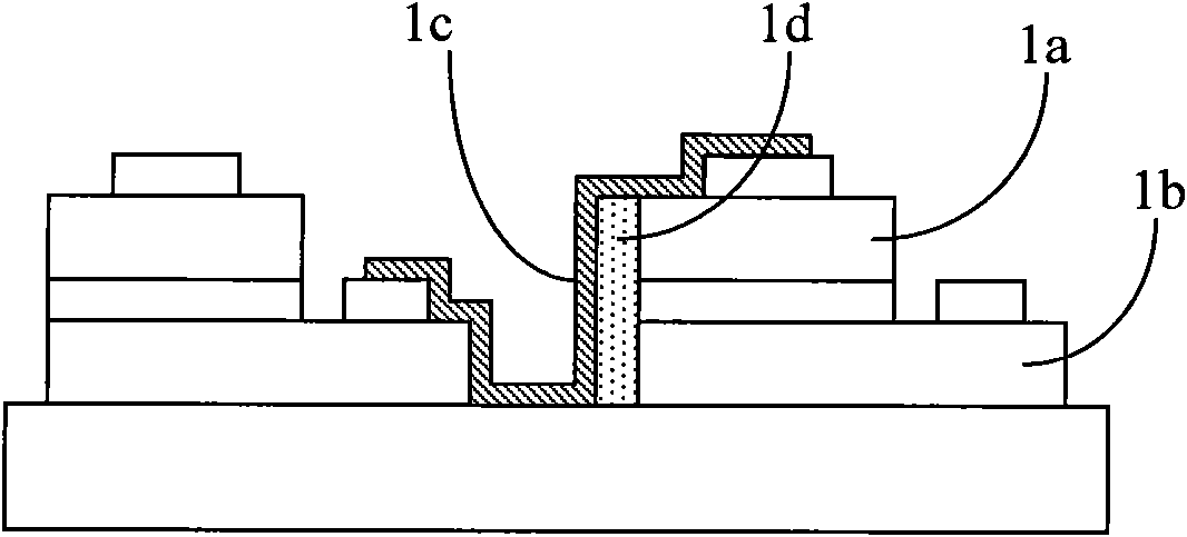
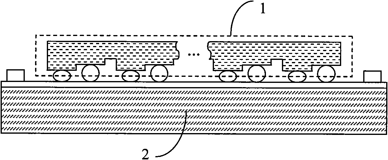
[0034] The LED chip 1 of the light-emitting device in this embodiment has nine light-emitting units 101 connected in series. Physically, the nine light-emitting units 101 are distributed into three rows and three columns on the LED chip 1 . Each light emitting unit 101 has a P pole and an N pole respectively, the surface of the P pole is covered with the P pole solder ball 102 , and the surface of the N pole is covered with the N pole solder...

Embodiment 2

[0046] see Figure 8 , which is a top view of the surface structure of the substrate of Example 2 of the light-emitting device of the present invention. Embodiment 2 of the present invention is substantially the same as Embodiment 1, the only difference being that the LED chip 1 is flip-chip mounted on the substrate 2, each light emitting unit 101 is electrically connected to the metal wire layer 203 on the substrate 2, and Through the metal wire layer 203 , the mixed connection of three parallels and three strings is realized.

[0047] It can be deduced that the present invention can realize the change of the electrical connection between the multiple light emitting units 101 on the LED chip 1 only by changing the wiring of the metal wire layer 203 on the substrate 2 .

[0048] In addition, the present invention can also have various modified embodiments. For example, the bump solder balls can be arranged on the upper surface of the metal pad of the substrate, or can be arra...


PUM


Abstract

The invention relates to a luminescent device formed by an inverted luminous cell array, which comprises an LED chip and a substrate. The LED chip is provided with a plurality of luminous cells which are insulated from each other, wherein each luminous cell is respectively provided with at least one of P poles and at least one of N poles. The upper surface of the substrate is provided with a metal wire layer. The LED chip is inverted on the substrate, the P poles and the N poles of each luminous cell on the LED chip are respectively and electrically connected with the metal wire layer on the substrate, and each luminous cell is connected with each other in series or in parallel by the metal wire layer. Compared with the prior art, the luminescent device replaces the metal wire on the LED chip with the metal wire layer on the substrate to realize that each luminous cell can be connected with each other in series or in parallel, thereby overcoming the technical difficulty that the wires among the luminous cells which are isolated from each other are hard to connect with each other in the normal technology. Furthermore, only by changing the design of the metal wire layer of the substrate, the luminescent device can realize the different designs such as the series connection, the parallel connection or the mixed connection, and is simple and flexible in technology relatively.

Description

technical field [0001] The invention belongs to the field of manufacturing light-emitting devices, and relates to a light-emitting device composed of flip-chip light-emitting unit arrays and a manufacturing method thereof. Background technique [0002] Light-emitting diode (LED) light sources have the advantages of high efficiency, long life, and no harmful substances such as Hg. With the rapid development of LED technology, the brightness and lifespan of LEDs have been greatly improved, making the application of LEDs more and more extensive. From outdoor lighting such as street lamps to indoor lighting such as decorative lamps, they are all used or replaced one after another. into LED as light source. [0003] Compared with a single large-size LED chip, in the case of the same chip area, the LED chip composed of multiple LED light-emitting unit arrays has the following advantages: the required driving current is small, the driving voltage is high, and the power supply of s...

Claims


Application Information

Patent Timeline
Patent Type & Authority Applications(China)
IPC IPC(8): H01L27/14H01L33/48H01L33/62H01L33/00
CPCH01L2224/14
Inventor 周玉刚肖国伟姜志荣曾照明赖燃兴许朝军
Owner APT ELECTRONICS
Why Eureka
Try Eureka