Three-dimensional light-emitting device formed by inverted light-emitting unit array and manufacturing method of three-dimensional light-emitting device

A technology of light-emitting units and light-emitting devices, which is applied in the direction of electric solid-state devices, semiconductor devices, electrical components, etc., to achieve the effects of simple process, elimination of process difficulties, and elimination of the preparation of silicon substrates

Inactive Publication Date: 2014-01-29
JIANGSU MICRO WAVE ELECTRONICS TECH
View PDF7 Cites 4 Cited by
  • Summary
  • Abstract
  • Description
  • Claims
  • Application Information

AI Technical Summary

Problems solved by technology

figure 2 It is a cross-sectional view of the LED chip structure in this technology. However, the substrate used needs to be prepared indepe

Method used


Image

  • Three-dimensional light-emitting device formed by inverted light-emitting unit array and manufacturing method of three-dimensional light-emitting device
  • Three-dimensional light-emitting device formed by inverted light-emitting unit array and manufacturing method of three-dimensional light-emitting device
  • Three-dimensional light-emitting device formed by inverted light-emitting unit array and manufacturing method of three-dimensional light-emitting device

Examples


Embodiment 1

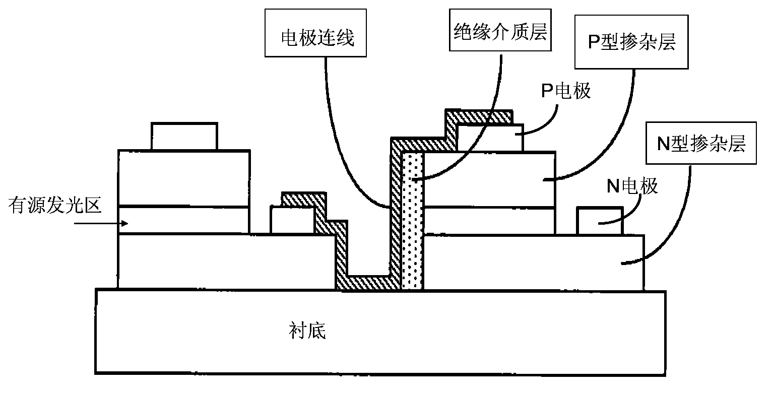
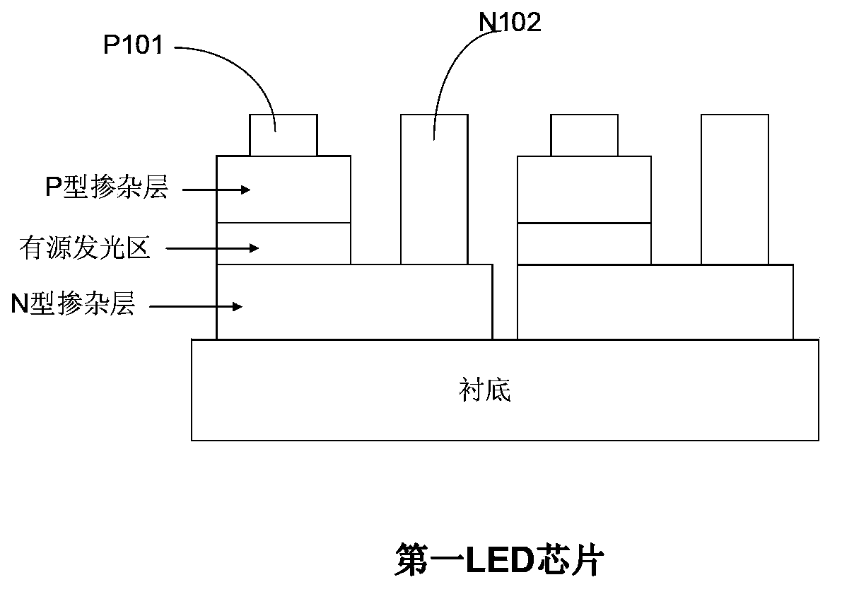
[0066] Please also see Figure 3 to Figure 7 , the three-dimensional light-emitting device in this embodiment consists of two LED light-emitting units of the first LED chip and three LED light-emitting units of the second LED chip to form a light-emitting array with five light-emitting units connected in series.

[0067] in, image 3 is a schematic cross-sectional view of the basic structure of the first LED chip; Figure 4 is a cross-sectional view of the basic structure of the second LED chip; Figure 5 It is a cross-sectional view of the basic structure of the three-dimensional light emitting device of the present invention after the first LED chip and the second LED chip are flip-chip connected; Image 6 It is a schematic diagram of the basic circuit of the three-dimensional light-emitting device of the present embodiment; Figure 7 The above is a schematic diagram of the layout design of the first LED chip, Figure 7 The following is a schematic diagram of the layout ...

Embodiment 2

[0073] Please also see Figure 3 to Figure 5 and Figure 8 , Figure 9 , the three-dimensional light-emitting device in this embodiment can be regarded as the series-parallel array structure of this embodiment formed by the two LED series arrays in Embodiment 1.

[0074] in, image 3 is a schematic cross-sectional view of the basic structure of the first LED chip; Figure 4 is a schematic cross-sectional view of the basic structure of the second LED chip; Figure 5 It is a schematic cross-sectional view of the basic structure of the three-dimensional light-emitting device of the present invention after the first LED chip and the second LED chip are flip-chip connected; Figure 8 It is a schematic diagram of the basic circuit of the three-dimensional light-emitting device of the present embodiment; Figure 9 The above is a schematic diagram of the layout design of the first LED chip, Figure 9 The following is a schematic diagram of the layout design of the second LED chi...

Embodiment 3

[0080] Please also see Figure 4 ,and Figure 10 to Figure 13 , the three-dimensional light-emitting device in this embodiment can be regarded as a light-emitting array with four light-emitting units connected in series consisting of one LED light-emitting unit and one independent area of ​​the first LED chip and three LED light-emitting units of the second LED chip .

[0081] in, Figure 10 is a schematic cross-sectional view of the basic structure of the first LED chip; Figure 4 is a schematic cross-sectional view of the basic structure of the second LED chip; Figure 11 It is a schematic cross-sectional view of the basic structure of the three-dimensional light-emitting device of the present invention after the first LED chip and the second LED chip are flip-chip connected; Figure 12 It is a schematic diagram of the basic circuit of the three-dimensional light-emitting device of the present embodiment; Figure 13 The above is a schematic diagram of the layout design ...


PUM


Abstract

Disclosed are a stereo light-emitting device composed of a flip-chip light-emitting unit array and a manufacturing method therefor. By substituting a flip-chip connection of a P-N complementary light-emitting diode (LED) chip for the metal wiring on the LED chip, the stereo light-emitting device realizes a series/parallel connection between individual light-emitting units, so as to completely eliminate the process difficulty of wiring on an LED chip trench, greatly improving the production yield and simultaneously obviating the preparation of a silicon substrate in the conventional flip-chip process. Furthermore, different series connection, parallel connection or series/parallel connection designs can be realized only by changing the layout design of an LED chip, the process is relatively simple and flexible, and the production efficiency can be greatly improved.

Description

technical field [0001] The invention belongs to the field of manufacturing light-emitting devices, in particular to a three-dimensional light-emitting device composed of a light-emitting unit array prepared by a flip-chip process and a manufacturing method thereof. Background technique [0002] Light-emitting diode (LED) light sources have the advantages of high efficiency, long life, and no harmful substances such as Hg. With the rapid development of LED technology, the brightness and lifespan of LEDs have been greatly improved, making the application fields of LEDs more and more extensive, from outdoor lighting such as street lights to indoor lighting such as decorative lights and general lighting. Use or replace with LED as light source. [0003] Compared with a single large-size LED chip, in the case of the same chip area, the LED chip composed of multiple LED light-emitting unit arrays has the following advantages: the required driving current is small, the driving vol...

Claims


Application Information

Patent Timeline
IPC IPC(8): H01L27/15H01L33/62
CPCH01L25/0756H01L33/62H01L2924/0002H01L2924/00
Inventor 许玉方
Owner JIANGSU MICRO WAVE ELECTRONICS TECH
Why Eureka
Try Eureka