Contact image sensor

An image sensor and contact technology, which is applied in image communication, instruments, banknote authenticity inspection, etc., can solve the problems of unrecognizable color-changing ink anti-counterfeiting marks, etc., and achieves a product suitable for mass production, reasonable in structural design, and small in size Effect

Active Publication Date: 2011-03-16
WEIHAI HUALING OPTO ELECTRONICS CO LTD
View PDF7 Cites 19 Cited by
  • Summary
  • Abstract
  • Description
  • Claims
  • Application Information

AI Technical Summary

Problems solved by technology

[0005] The technical problem to be solved by the present invention is: since the existing contact image sensor cannot recognize the color-changing ink anti-counterfeiting mark on the surface of banknotes, a contact image sensor with two light sources with different light-emitting angles on both sides of the lens is proposed. The contact image sensor can be used to identify the color-changing ink anti-counterfeiting mark on the surface of banknotes, so as to effectively identify the authenticity of banknotes

Method used


Image

  • Contact image sensor
  • Contact image sensor
  • Contact image sensor

Examples


Embodiment 1

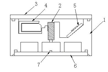
[0020] Embodiment 1: as image 3 As shown in the figure, the frame 1, the lens 2, the light-transmitting plate 3, the light guide strip structured light source 4, the LED array structured light source 5, the circuit board accommodating the photoelectric conversion chip 6, the photoelectric conversion chip 7, and the non-reflective film 8 are marked. For example, the light sources on both sides of the lens are light guide strip structure and LED array structure respectively. The two light sources have different luminous angles. The luminous angles of the two light sources can be adjusted according to the needs. The luminous angle of one of the light sources can be adopted relative to the lens axis. An angle of 20° or 30°, the light emitting angle of another light source can adopt an angle of 60° to 80° relative to the axis of the lens.

Embodiment 2

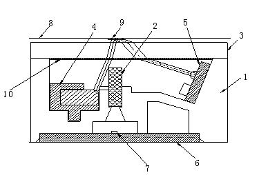
[0021] Embodiment 2: as Figure 4 As shown in the figure, the frame 1, the lens 2, the light-transmitting plate 3, the light guide strip structured light source 4, the light guide strip structured light source 5, the circuit board containing the photoelectric conversion chip 6, the photoelectric conversion chip 7, and the non-reflective film 8, this The light sources on both sides of the lens in the embodiment adopt a light guide strip structure. The two light sources have different light emitting angles. The light emitting angles of the two light sources can be adjusted according to the needs. The light emitting angle of one of the light sources can be 20° or 20° relative to the axis of the lens. For an angle of 30°, the light emitting angle of the other light source can adopt an angle of 60° to 80° relative to the axis of the lens.

Embodiment 3

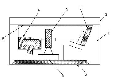
[0022] Embodiment 3: as Figure 5 As shown in the figure, the frame 1, the lens 2, the light-transmitting plate 3, the LED array structure light source 4, the LED array structure light source 5, the circuit board 6 accommodating the photoelectric conversion chip, the photoelectric conversion chip 7, and the non-reflective film 8 are marked. For example, the light sources on both sides of the lens adopt LED array structure. The two light sources have different light angles. The light angles of the two light sources can be adjusted according to the needs. The light angle of one light source can be 20° or 30° relative to the lens axis. The light emitting angle of another light source can be 60° to 80° relative to the axis of the lens.


PUM


Abstract

The invention relates to a contact image sensor (CIS), belonging to the technical field of image readout devices. The invention is used for identifying the color-changing ink anti-counterfeiting label on the surface of the paper money. The CIS is characterized in that light sources different in light-emitting angles are respectively arranged at the two sides of a lens; and a non-reflecting film is adhered to the inner surface of a transparent board. As the color-changing ink anti-counterfeiting label on the surface of the genuine paper money changes in different colors from different angles, that is, the light irradiates the color-changing ink anti-counterfeiting label on the surface of the genuine paper money in different angles and the reflected light is different, but the counterfeit paper money does not have the characteristic, the light emitted by the two light sources of the CIS respectively irradiates the color-changing ink anti-counterfeiting label on the surface of the paper money in different angles, the reflected light is respectively received by the CIS, the CIS analyzes, processes and compares the two kinds of light received by the CIS and the obtained information is compared with the relevant information of the genuine paper money so as to achieve the aim of identifying authenticity of the paper money.

Description

technical field [0001] The invention relates to an image reading device, in particular to a contact image sensor for identifying the color-changing ink anti-counterfeiting mark on the surface of banknotes. Background technique [0002] figure 1 2 is a lens, 4 and 5 are two light sources with the same light emitting angle, 7 is a photoelectric conversion chip (photosensitive integrated circuit) that receives light collected by lens 2, and 6 is a Carry the circuit board of photosensitive integrated circuits 7 arranged in a line, 1 is the frame that accommodates light source 4 and light source 5, lens 2, circuit board 6, 3 is the light-transmitting board that is arranged on the frame 1 and carries original. [0003] There are two types of light source settings for the existing contact image sensor, one is a light guide strip light source, and the other is an LED array light source. irradiates the original at an angle. [0004] The above-mentioned contact image sensor has the...

Claims


Application Information

Patent Timeline
Patent Type & Authority Applications(China)
IPC IPC(8): G07D7/12H04N1/028
Inventor 戚务昌宋荣鑫王萍
Owner WEIHAI HUALING OPTO ELECTRONICS CO LTD
Why Eureka
Try Eureka