Al technical title is built by PatSnap Al team. It summarizes the technical point description of the patent document.
A manufacturing method and laser technology, which are applied to the structure of optical waveguide semiconductors and other directions, can solve the problems of nonlinear bending, difficult shaping, and vertical asymmetry of the light-emitting position, and achieve the effect of avoiding direct contact and reducing thermal stress.
Inactive Publication Date: 2011-03-30
Shandong Huaguang Optoelectronics Co. Ltd.
View PDF6 Cites 4 Cited by
Summary
Abstract
Description
Claims
Application Information
AI Technical Summary
This helps you quickly interpret patents by identifying the three key elements:
Problems solved by technology
Method used
Benefits of technology
Problems solved by technology
[0005] The present invention aims at the problems of asymmetry in the vertical direction of the light-emitting position, nonlinear bending, and difficulty in shaping existing in the existing semiconductor laser bar packaging technology, and provides a method that can make the light-emitting poi
Method used
Image
Click on the blue label to locate the original text in one second.
Reading with bidirectional positioning of images and text.
Examples
Embodiment Construction
[0019] Semiconductor laser bar manufacturing method of the present invention, concrete steps are as follows:
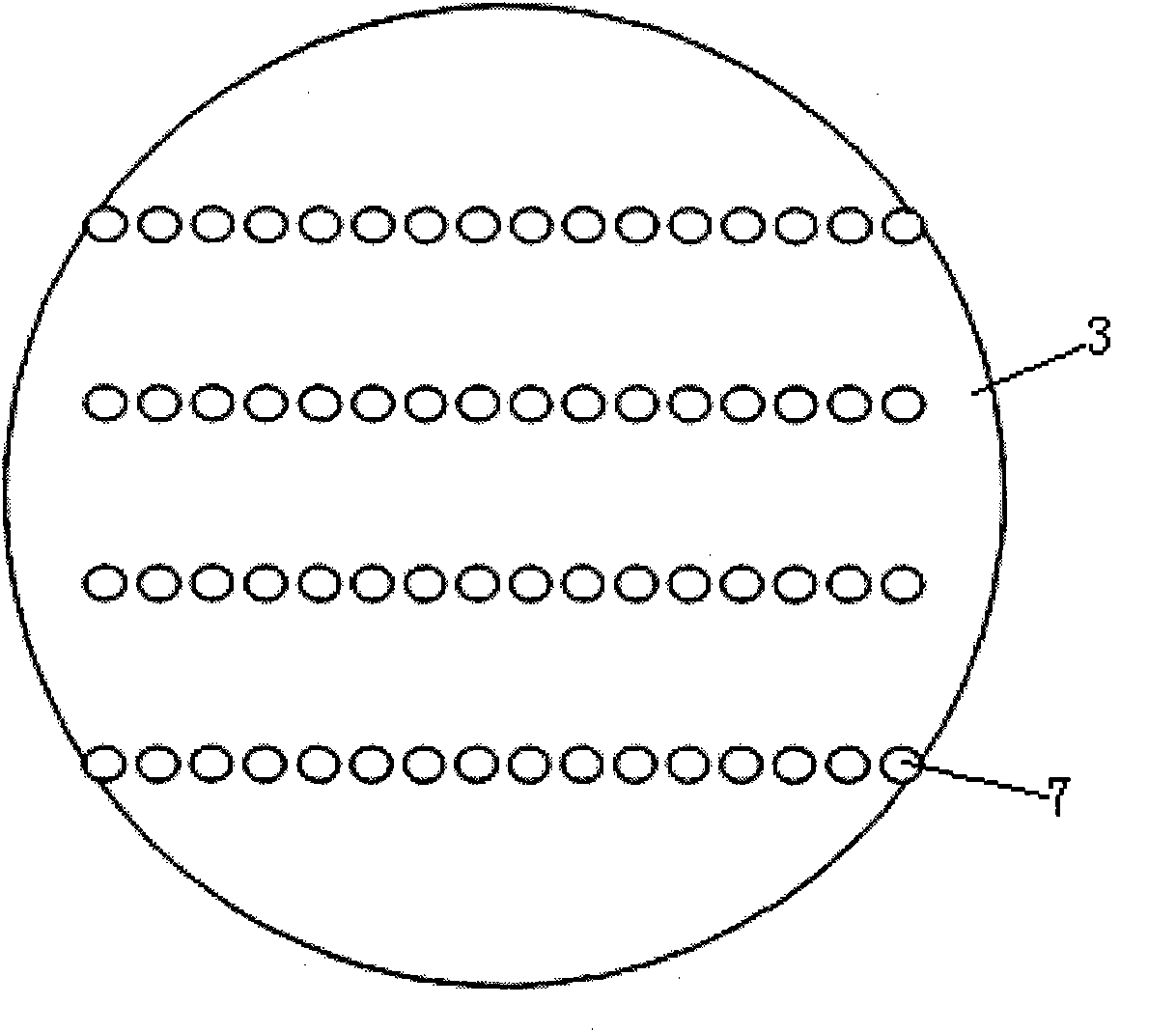
[0020] (1) if figure 1 As shown, holes are drilled on a wafer 3 with a thickness of 80 microns-100 microns, and the row spacing of the punched holes 7 on the wafer 3 is 1.2mm (different sizes from 0.8mm to 4mm can be set according to the laser cavity length), and the column spacing 10mm (different sizes from 4mm to 20mm can be set according to the length of the bar). The thickness of the wafer 3 is set at 80 microns-100 microns to facilitate the realization that the light-emitting area after bonding is just in the center of the bonded wafer. The wafer thickness can also be adjusted according to the thickness of the semiconductor laser epitaxial wafer. The material of the wafer is an insulating heat conductor , including GaAs, single crystal Si, SiC or diamond, etc.; the perforated hole 7 on the wafer can be a columnar hole or a row of holes, and its spacing is relate...
PUM
Abstract
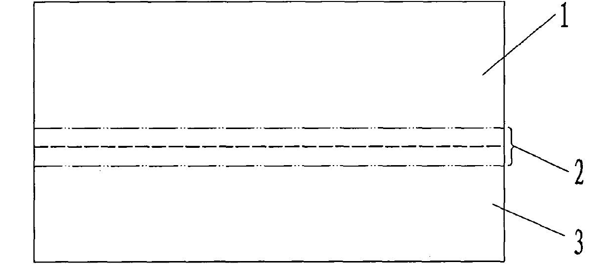
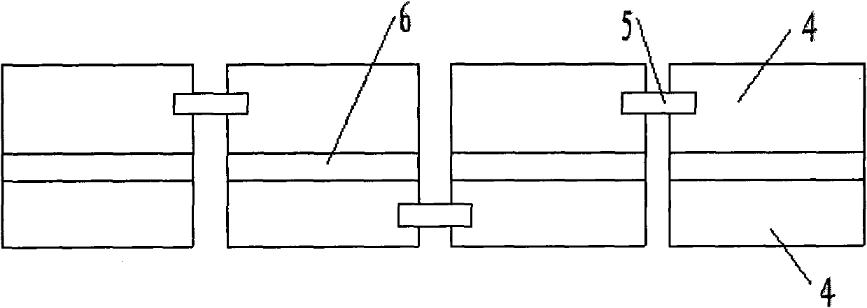
The invention provides a method for manufacturing a semiconductor laser bar, which comprises the following steps of: (1) before bar decomposition, allowing a semiconductor laser epitaxial wafer and a wafer of which the double sides are metalized to form a gold-gold alloy through a bonding machine, and ensuring that the dimension of the wafer of which the double sides are metalized is the same as that of the semiconductor laser epitaxial wafer but the thickness is smaller than that of the semiconductor laser epitaxial wafer so as to guarantee that a luminous zone is positioned at a central position of a die on the rear of the alloy; (2) decomposing the alloyed semiconductor laser epitaxial wafer according to required width; (3) plating corresponding film systems on a front cavity surface and a rear cavity surface of the bar; and (4) packaging according to the conventional linear packaging process. Through the method, the luminous zone of the bar of the semiconductor laser is moved to the inside of the die, so the high-temperature P zone is prevented from directly contacting a solder, the thermal stress is reduced, luminous points of each bar form a strict line in the linear packaging process, the nonlinear bending is reduced, and a shaping process with higher requirement is realized.
Description
technical field [0001] The invention relates to a method for manufacturing high-power laser diode bars, and belongs to the technical field of bar manufacturing. Background technique [0002] In the 1960s, with the advent of lasers, laser technology has been widely used in various fields. Among them, semiconductor lasers have the advantages of small size, light weight, high efficiency, long life, easy modulation and low price, and have been widely used in industry, medicine and military fields, such as material processing, optical fiber communication, laser ranging, target indication , laser guidance, laser radar, space optical communication, etc. In particular, high-power bar semiconductor lasers are packaged linearly and used in side-pumped solid gain media, and the optical power has reached a level of more than 600W in a single linear array; packaged into a stacked bar array, the power has reached the order of 10,000 W, and the bar array It has become an important packag...
Claims
Application Information
Patent Timeline
Application Date:The date an application was filed.
Publication Date:The date a patent or application was officially published.
First Publication Date:The earliest publication date of a patent with the same application number.
Issue Date:Publication date of the patent grant document.
PCT Entry Date:The Entry date of PCT National Phase.
Estimated Expiry Date:The statutory expiry date of a patent right according to the Patent Law, and it is the longest term of protection that the patent right can achieve without the termination of the patent right due to other reasons(Term extension factor has been taken into account ).
Invalid Date:Actual expiry date is based on effective date or publication date of legal transaction data of invalid patent.
