Method for improving critical dimension uniformity of mask

A critical dimension and uniformity technology, applied in the field of silicon semiconductor devices, can solve the problem of reduced uniformity of the critical dimension of the mask, and achieve the effect of improving the uniformity

Inactive Publication Date: 2011-04-20
SEMICON MFG INT (SHANGHAI) CORP
View PDF0 Cites 0 Cited by
  • Summary
  • Abstract
  • Description
  • Claims
  • Application Information

AI Technical Summary

Problems solved by technology

[0003] The purpose of the present invention is to provide a method for improving the uniformity of critical dimension of a mask, so as to solve the problem in the prior art that the uniformity of critical dimension of a mask is reduced due to the manufacturing process of the mask

Method used


Image

  • Method for improving critical dimension uniformity of mask
  • Method for improving critical dimension uniformity of mask
  • Method for improving critical dimension uniformity of mask

Examples


Embodiment Construction

[0020] In order to make the purpose and features of the present invention more comprehensible, the specific implementation manners of the present invention will be further described below in conjunction with the accompanying drawings.

[0021] As mentioned in the background art, there are many factors affecting the CD uniformity of the mask during the mask manufacturing process, resulting in low CD uniformity of the mask.

[0022] The core idea of ​​the present invention is to improve the uniformity of the critical dimension of the mask by feeding back the difference distribution of critical dimension of the mask to the photolithography step in the mask manufacturing process, and then adjusting the photolithography energy distribution of the photolithography step.

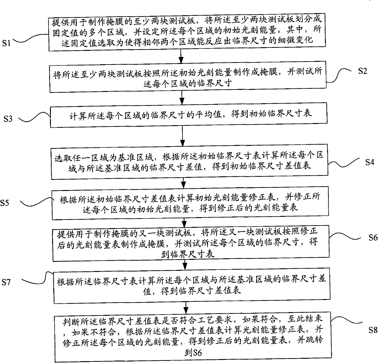
[0023] figure 2 It is a flowchart of a method for improving mask critical dimension uniformity according to the present invention, including:

[0024] S1: Provide at least two test boards for making masks, divide...


PUM


Abstract

The invention provides a method for improving critical dimension uniformity of a mask. The differential distribution of critical dimension of the mask is fed back to a photoetching step in a mask manufacturing process, so that the photoetching energy distribution in the photoetching step is adjusted, and the aim of improving the critical dimension uniformity of the mask is fulfilled.

Description

technical field [0001] The invention relates to the technical field of silicon semiconductor devices, in particular to a method for improving mask critical dimension uniformity (critical dimension uniformity, CDU). Background technique [0002] As the critical dimension on the wafer continues to shrink, the requirement for the accuracy of the critical dimension of the mask (mask) is getting higher and higher, and the CDU of the mask is an important measurement index. Generally, in the manufacturing process of the mask, a transparent substrate is provided first, and a metal layer is formed on the transparent substrate, and then a photoresist layer is formed on the metal layer. The resist layer is removed to expose the metal layer under the removed photoresist layer. Afterwards, the exposed metal layer is etched away by dry etching or wet etching. After the photoresist layer is completely removed, light-shielding and light-transmitting patterns are formed on the transparent ...

Claims


Application Information

Patent Timeline
Patent Type & Authority Applications(China)
IPC IPC(8): G03F1/14G03F1/36
Inventor 陈明
Owner SEMICON MFG INT (SHANGHAI) CORP
Why Eureka
Try Eureka