Semiconductor structure and formation method thereof

a technology of semiconductor devices and structure, applied in the field of semiconductor manufacturing, can solve problems affecting the consistency of electrical properties of formed semiconductor devices, and achieve the effects of reducing width dimension differences, improving critical dimension (cd) uniformity of target pattern layers in each region, and reducing width of opening of pattern isolated regions

Active Publication Date: 2021-03-23
SEMICONDUCTOR MANUFACTURING INTERNATIONAL (BEIJING) CORP +1
View PDF2 Cites 0 Cited by
  • Summary
  • Abstract
  • Description
  • Claims
  • Application Information

AI Technical Summary

Benefits of technology

[0006]One problem to be addressed by embodiments and implementations of the present disclosure is to provide a semiconductor structure and a formation method thereof, which improve the uniformity of critical dimensions of a target pattern layer in each region.
[0009]Compared with the prior art, a technical solution in some embodiments and implementations of the present disclosure have the following advantages:
[0010]In some embodiments and implementations of the present disclosure, the base is formed with a plurality of separate hard mask layers. After the adjacent hard mask layers and the base define an opening, a trimming layer at least on a side wall of the opening of the pattern isolated region is formed, where the trimming layer and the hard mask layer constitute a mask structure layer. As the opening is wider, the lateral etching of the base is more severe, and the formed target pattern layer is narrower. By means of the trimming layer, the width of the opening of the pattern isolated region is reduced, thereby reducing a width dimension difference between the openings of the pattern isolated region and the pattern dense region. In the step of subsequently etching a portion of the thickness of the base exposed by the opening, the trimming layer can compensate a difference of lateral etching quantities of the base corresponding to the pattern isolated region and the pattern dense region. Correspondingly, after forming a plurality of target pattern layers protruding from the remaining base, the critical dimension (CD) uniformity of the target pattern layer in each region is improved.

Problems solved by technology

Moreover, the difference between the pattern critical dimensions of a pattern dense region and a pattern isolated region affects the consistency of the electrical properties of the formed semiconductor devices.

Method used


Image

  • Semiconductor structure and formation method thereof
  • Semiconductor structure and formation method thereof
  • Semiconductor structure and formation method thereof

Examples


Embodiment Construction

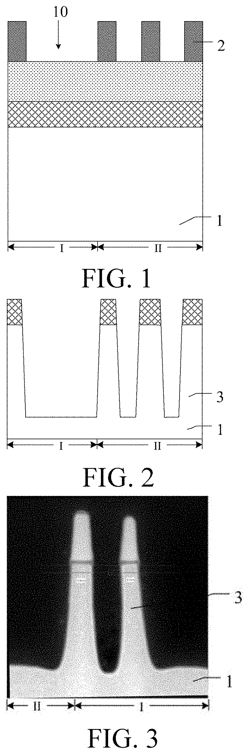
[0016]At present, critical dimension uniformity of a pattern dense region and a pattern isolated region is poor. A method for forming a semiconductor structure is now discussed to analyze a reason why the critical dimension uniformity of a pattern dense region and a pattern isolated region is poor.

[0017]FIG. 1 and FIG. 2 schematically show structure diagrams corresponding to various steps in a method for forming a semiconductor structure.

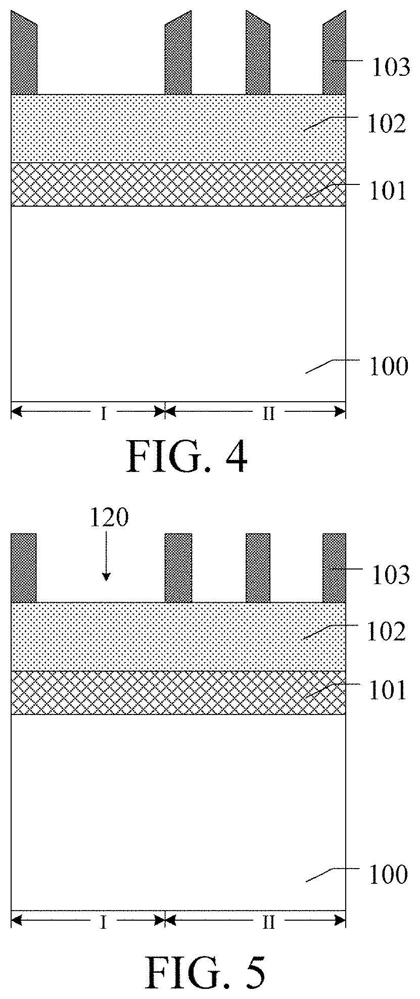
[0018]Referring to FIG. 1, a base 1 is provided, the base 1 including a pattern dense region II and a pattern isolated region I.

[0019]The base 1 is formed with a plurality of separate hard mask layers 2. Adjacent hard mask layers 2 and the base 1 define an opening 10, where the opening 10 of the pattern isolated region I is wider than the opening 10 of the pattern dense region II.

[0020]Referring to FIG. 2, by using the mask structure layer 2 (as shown in FIG. 1) as a mask, a portion of the thickness of the base1 exposed by the opening 10 is etched t...


PUM

PropertyMeasurementUnit
thicknessaaaaaaaaaa
bias poweraaaaaaaaaa
semiconductor structureaaaaaaaaaa

Abstract

A semiconductor structure and a formation method thereof are provided. The formation method includes: providing a base, the base including a pattern dense region and a pattern isolated region; forming a plurality of separate hard mask layers on the base, where adjacent hard mask layers and the base define an opening, and an opening of the pattern isolated region is wider than an opening of the pattern dense region; forming a trimming layer at least on a side wall of the opening of the pattern isolated region, the trimming layer and the hard mask layer constituting a mask structure layer; and etching, using the mask structure layer as a mask, a portion of the thickness of the base exposed by the opening to form a plurality of target pattern layers protruding from the remaining base. Embodiments and implementations of the present disclosure are advantageous for improving a critical dimension uniformity of a target pattern layer in each region.

Description

RELATED APPLICATIONS[0001]The present application claims priority to Chinese Patent Appln. No. 201910152105.1, filed Feb. 28, 2019, the entire disclosure of which is hereby incorporated by reference.BACKGROUNDTechnical Field[0002]Embodiments and implementations of the present disclosure relate to the field of semiconductor manufacturing, and in particular, to a semiconductor structure and a formation method thereof.Related Art[0003]In a semiconductor integrated circuit manufacturing process, a series of procedures such as deposition, photolithography, etching, and planarization processes may be used to form a semiconductor structure. Photolithography and etching are main patterning means during semiconductor manufacturing.[0004]The photolithography process generally includes: forming a photosensitive material layer (for example, a photoresist layer) on a base, and then transferring a pattern on a mask onto the photosensitive material layer by exposure, thereby forming a pattern in t...

Claims


Application Information

Patent Timeline
Patent Type & Authority Patents(United States)
IPC IPC(8): H01L21/308H01L21/3065H01L21/02H01L29/06H01L21/311H01L21/027H01L21/033
CPCH01L21/3086H01L21/0223H01L21/3065H01L21/3081H01L21/3088H01L21/31116H01L29/0657H01L21/0234H01L21/0271H01L21/02118H01L21/02164H01L21/02252H01L21/02274H01L21/02326H01L21/033H01L21/0212H01L21/823431
Inventor ZHANG, HAIYANGZHENG, ERHU
Owner SEMICONDUCTOR MANUFACTURING INTERNATIONAL (BEIJING) CORP
Why Eureka
Try Eureka