Method for manufacturing self-aligned double pattern and method for manufacturing semiconductor device

A technology of dual graphics and manufacturing methods, applied in semiconductor/solid-state device manufacturing, electrical components, circuits, etc., can solve problems that are not good, affect the performance and yield of semiconductor devices, and achieve improved morphology, accurate graphic features, and precise effect

Active Publication Date: 2021-10-01
SEMICON MFG INT (SHANGHAI) CORP +1
View PDF3 Cites 0 Cited by
  • Summary
  • Abstract
  • Description
  • Claims
  • Application Information

AI Technical Summary

Problems solved by technology

[0003] However, when the integrated circuit chip technology enters the node of 7nm and below, the critical dimension uniformity (Critical dimension uniformity, CDU) of the pattern obtained on the target etching layer by using the self-aligned double patterning technology is not good, which seriously affects the manufacturing process. The performance and yield of semiconductor devices

Method used


Image

  • Method for manufacturing self-aligned double pattern and method for manufacturing semiconductor device
  • Method for manufacturing self-aligned double pattern and method for manufacturing semiconductor device
  • Method for manufacturing self-aligned double pattern and method for manufacturing semiconductor device

Examples


Embodiment Construction

[0043] A method of manufacturing a polysilicon gate using self-aligned double patterning (SADP) technology, comprising the following steps:

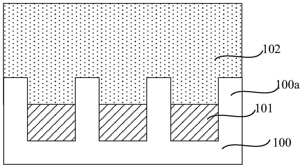
[0044] First, please refer to Figure 1A , providing a semiconductor substrate 100 having fins 100a and shallow trench isolation structures (STI) 101, the shallow trench isolation structures 101 are formed between adjacent fins 100a and the top of the shallow trench isolation structures 101 is lower than the fins On the top of the fin 100a, polysilicon (poly) is deposited on the surface of the fin 100a and the shallow trench isolation structure 101, the thickness of the deposited polysilicon layer is sufficient to fill the trench between adjacent fins 100a and between the fins having a sufficient thickness on top of the fin 100a, chemical mechanical planarization (CMP) is performed on the top of the deposited polysilicon to form a polysilicon layer 102 with a flat top surface and the desired thickness on top of the fin 100a;

[0045] Ne...


PUM


Abstract

The invention provides a method for manufacturing a self-aligned double pattern and a method for manufacturing a semiconductor device. Considering the negative influence of the process of the target etching layer formed on the semiconductor substrate, the data such as the thickness of the formed target etching layer is fed back In the subsequent process of etching the target etching layer, the etching effect of the target etching layer can be more accurately controlled, thereby improving the uniformity of the key dimensions of the pattern obtained on the target etching layer, and improving the obtained The performance and yield of the semiconductor device; further, considering the negative impact of the lithography process, the lithography process conditions are adjusted in time according to the critical dimensions after lithography and the thickness of the etch protection layer and cover layer, thereby improving the final core. The morphology of the mold is further improved to further improve the uniformity of the critical dimension of the pattern obtained on the target etching layer.

Description

technical field [0001] The invention relates to the technical field of integrated circuit manufacturing, in particular to a method for manufacturing a self-aligned double pattern and a method for manufacturing a semiconductor device. Background technique [0002] With the continuous shrinking of the minimum line width and spacing of integrated circuit design, when the feature size of the exposure line is close to the theoretical resolution limit of the exposure system, the lithographic imaging will be severely distorted, resulting in a serious decline in the quality of the lithographic pattern. . The application of self-aligned double patterning (Self-aligned Double Patterning, SADP) technology can greatly reduce the influence of optical proximity effect, and alleviate the problem of single pattern shrinkage, and realize smaller pattern feature size (Critical dimension, CD). [0003] However, when the integrated circuit chip technology enters the node of 7nm and below, the...

Claims


Application Information

Patent Timeline
Patent Type & Authority Patents(China)
IPC IPC(8): H01L21/033H01L21/3213
CPCH01L21/0337H01L21/32139
Inventor 张海洋刘少雄钟伯琛
Owner SEMICON MFG INT (SHANGHAI) CORP
Why Eureka
Try Eureka