
Method for fabricating a gate structure

A manufacturing method and gate structure technology, applied in semiconductor/solid-state device manufacturing, electrical components, transistors, etc., can solve problems such as increasing short circuits and/or component failures, degrading critical voltage and reliability, etc.

Inactive Publication Date: 2011-05-04
TAIWAN SEMICON MFG CO LTD
View PDF2 Cites 4 Cited by
  • Summary
  • Abstract
  • Description
  • Claims
  • Application Information

AI Technical Summary

Problems solved by technology

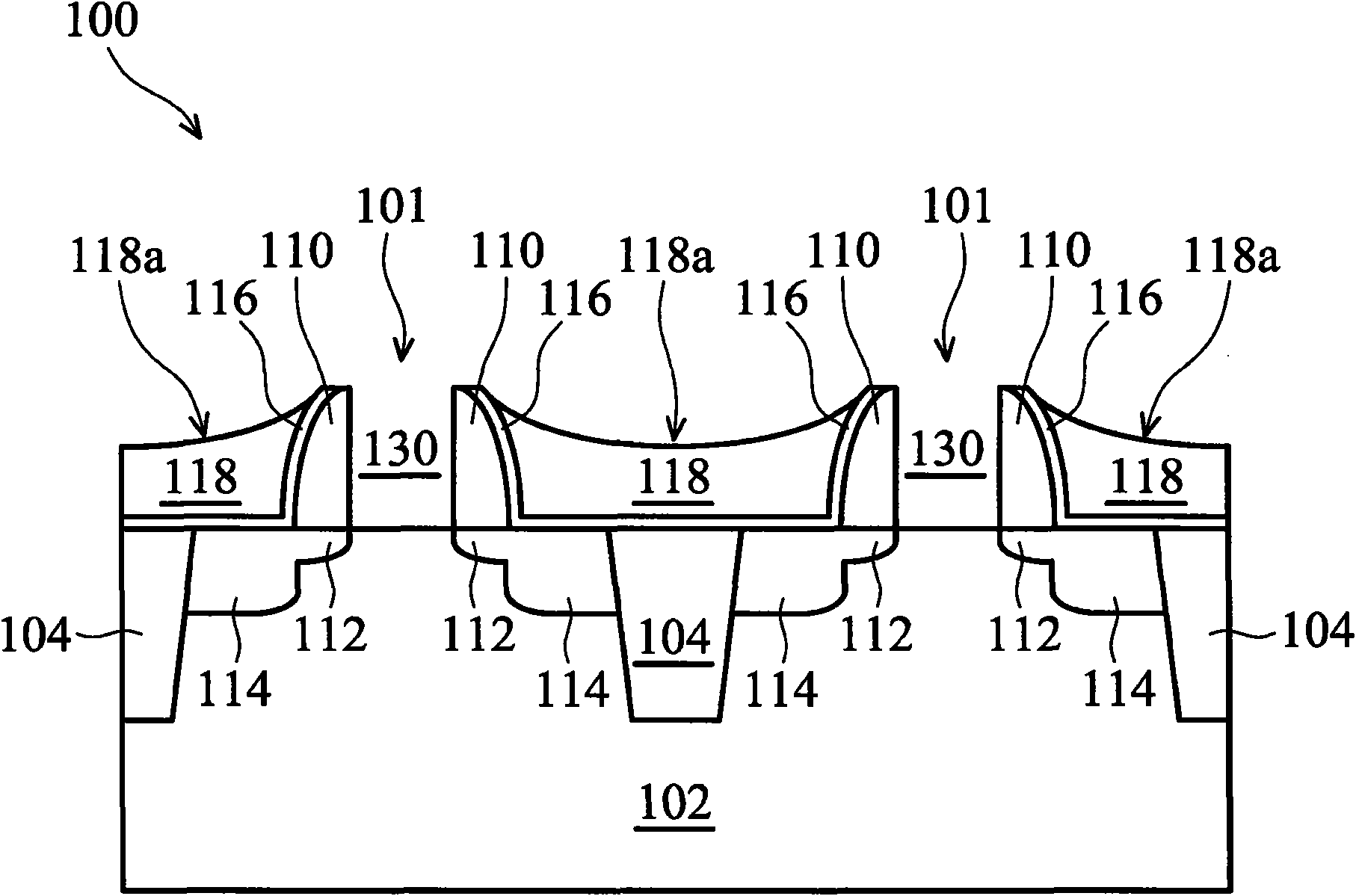
Therefore, characteristics such as threshold voltage and reliability will be degraded
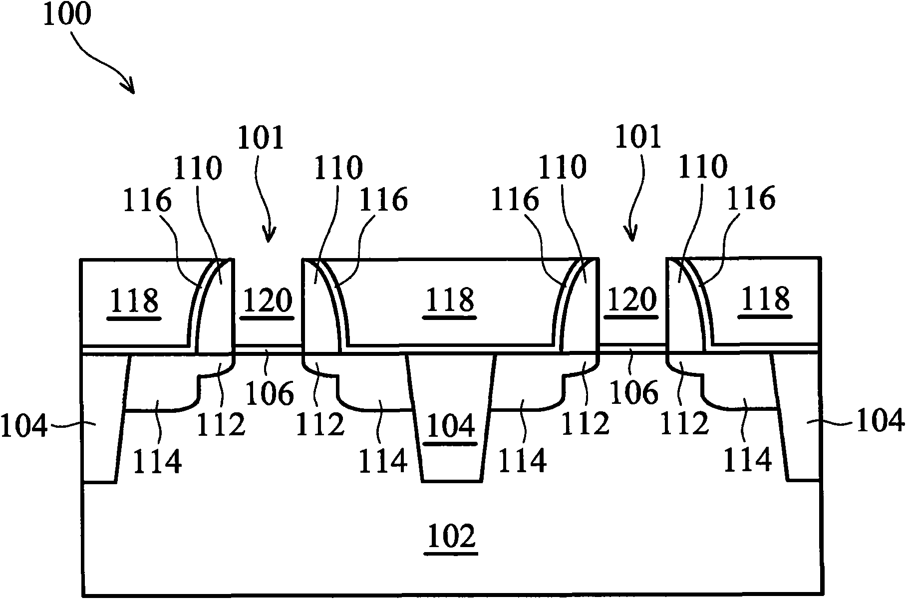
On the other hand, these notches 118a appearing in the interlayer dielectric layer 118 may become a metal receiving area in the subsequent process, thereby increasing the possibility of short circuit and / or device failure.

Method used


Image

  • Method for fabricating a gate structure
  • Method for fabricating a gate structure
  • Method for fabricating a gate structure

Examples


Embodiment Construction

[0055] It will be appreciated that the following provides a number of different embodiments or examples for achieving different features of the invention. Specific examples of elements or arrangements are described below to simply illustrate the present invention. Of course, these descriptions are only used as examples and not intended to limit the scope of the present invention. For example, the description of "forming a first element on or over a second element" includes the implementation of the direct contact between the first element and the second element, or includes the implementation of the first element and the second element An implementation in which additional elements are placed between elements such that the first element does not directly contact the second element. In addition, the present invention may reuse symbols and / or characters in different instances. Such repetition is for simplicity and clarity and is not intended to define the relationship between ...


PUM


Abstract

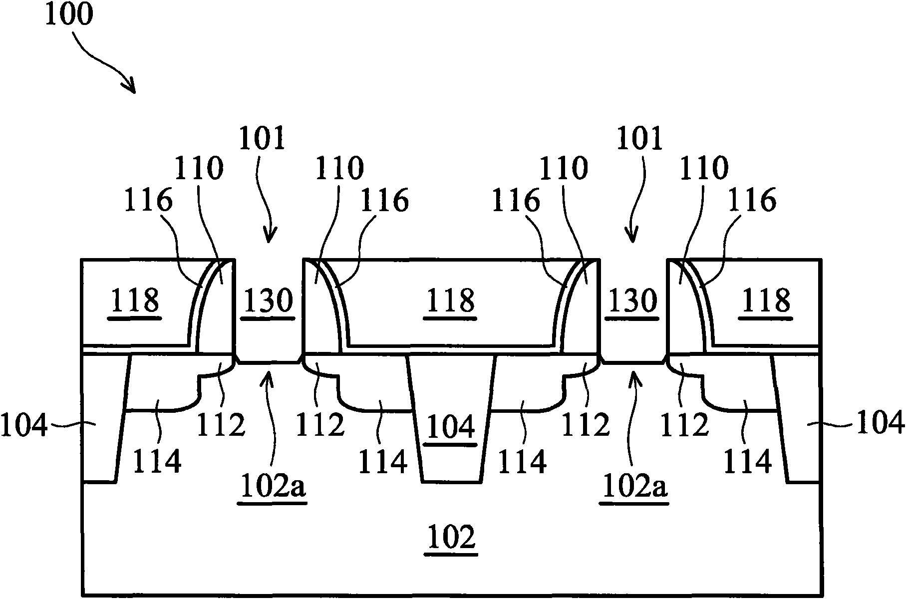
A method of fabricating the gate structure comprises: sequentially depositing and patterning a dummy oxide layer and a dummy gate electrode layer on a substrate; surrounding the dummy oxide layer and the dummy gate electrode layer with a nitrogen-containing dielectric layer and an interlayer dielectric layer; removing the dummy gate electrode layer; removing the dummy oxide layer by exposing a surface of the dummy oxide layer to a vapor mixture comprising NH3 and a fluorine-containing compound at a first temperature; heating the substrate to a second temperature to form an opening in the nitrogen-containing dielectric layer; depositing a gate dielectric; and depositing a gate electrode. The gate structure of the invention can be etched in the interlayer dielectric layer or the substrate without notches by dry chemistry.

Description

technical field [0001] The present invention relates to integrated circuit fabrication, and more particularly to semiconductor devices with gate structures. Background technique [0002] As the transistor size shrinks, the gate oxide thickness needs to be reduced to maintain performance as the gate length is reduced. However, in order to reduce the gate leakage current, a high-k gate oxide layer is used, which is at the same effective thickness as the general gate oxide used in future technology nodes. It may have a better physical thickness. [0003] In addition, when technology nodes shrink, in some integrated circuit designs, it is necessary to use metal gate electrodes instead of known polysilicon gate electrodes (poly gate electrodes) in order to improve the reduced features. Dimensions of performance of the device. One of the processes for forming the metal gate electrode is the "gate last" process, which allows the metal gate electrode to be prepared in the "last" ...

Claims


Application Information

Patent Timeline
Patent Type & Authority Applications(China)
IPC IPC(8): H01L21/28
CPCH01L21/2822H01L29/51H01L29/66545H01L29/6659H01L29/7833
Inventor 叶明熙黄益成徐帆毅欧阳晖
Owner TAIWAN SEMICON MFG CO LTD
Learn More