Eureka AIR delivers breakthrough ideas for toughest innovation challenges, trusted by R&D personnel around the world.

Method for making shallow channel isolation

A manufacturing method and technology of shallow trenches, which can be used in semiconductor/solid-state device manufacturing, electrical components, circuits, etc., and can solve the problems of semiconductor component operation, silicon oxide plug depression, affecting the electrical characteristics of semiconductor components, etc.

Inactive Publication Date: 2003-07-09
SILICON INTEGRATED SYSTEMS
View PDF0 Cites 3 Cited by
  • Summary
  • Abstract
  • Description
  • Claims
  • Application Information

AI Technical Summary

Problems solved by technology

[0003] However, in the process of removing the pad oxide layer formed by thermal oxidation, because the etching rate of silicon oxide deposited by chemical vapor deposition is greater than that of the pad oxide layer formed by thermal oxidation, it often causes The edge of the silicon oxide plug is dimpled
After the conductive material of the gate is subsequently deposited and the gate is defined, some conductive material is often left in the edge recess of the silicon oxide plug, which affects the electrical characteristics of the semiconductor device, such as the sub-threshold current. increase, etc., causing serious operational problems for various semiconductor components

Method used


Image

  • Method for making shallow channel isolation
  • Method for making shallow channel isolation
  • Method for making shallow channel isolation

Examples


Embodiment Construction

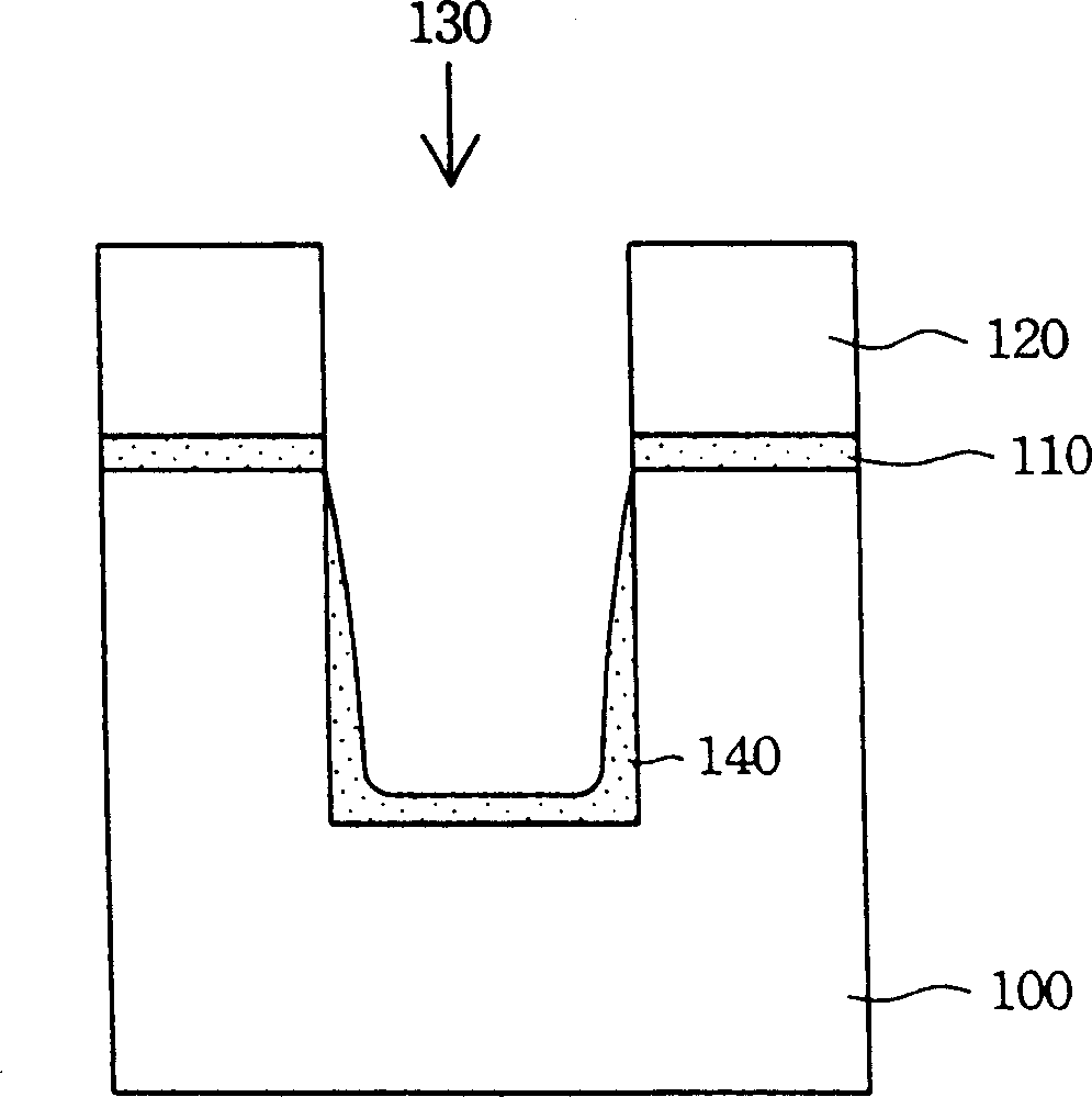
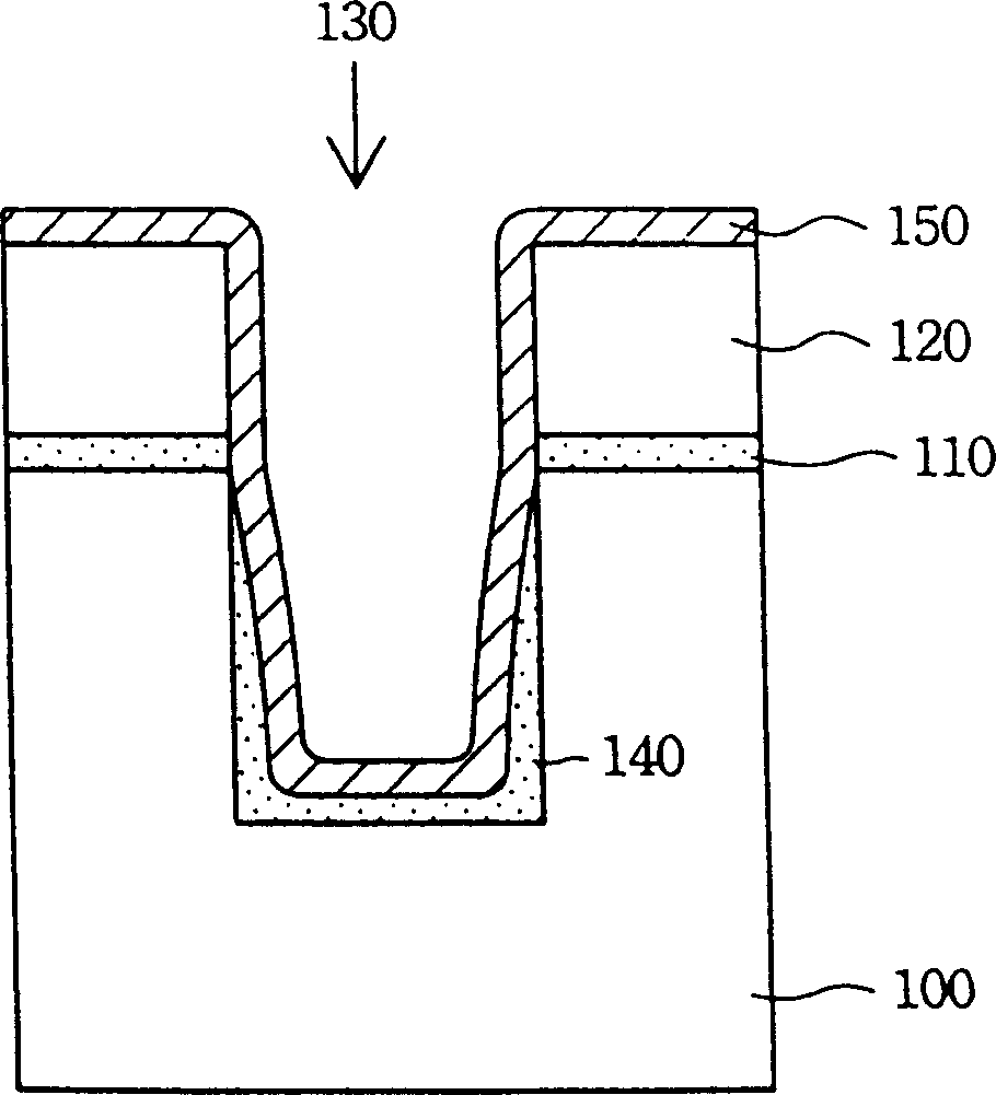
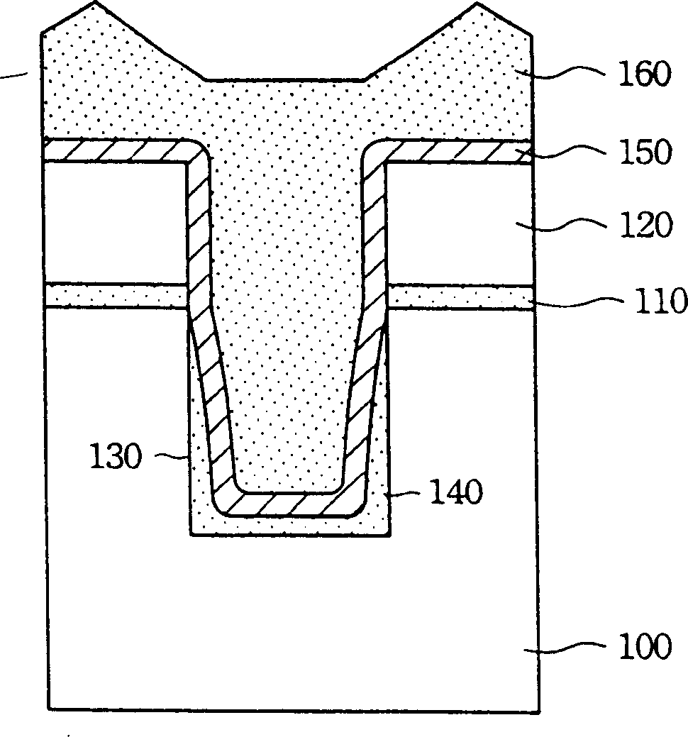
[0032] see Figure 1-5 , which shows a cross-sectional view of a manufacturing process of shallow trench isolation according to a preferred embodiment of the present invention.

[0033] figure 1 In this method, a pad oxide layer 110 and a silicon nitride layer 120 are sequentially formed on the substrate 100 first, and then a lithographic etching process is performed to pattern the silicon nitride layer 120 and the pad oxide layer 110 to expose part of the surface of the substrate 100 . Next, using the silicon nitride layer 120 as a mask, the exposed substrate 100 is etched to form a trench 130 in the substrate 100 .

[0034] A thermal oxidation method is then performed to form a liner oxide layer 140 on the surface of the trench 130 to repair the structural damage caused on the surface of the trench 130 during the etching process. Please note that the thickness of the liner oxide layer 140 formed on the top edge of the trench 130 is relatively thin, because of its geometry,...


PUM

PropertyMeasurementUnit
refractive indexaaaaaaaaaa

Abstract

The method for making shallow trench isolation at least includes the following steps: firstly, successively forming pad oxide layer and silicon nitride layer on the substrate, patterning silicon nitride layer and pad oxide layer to expose partial substrate surface, etching the exposed substrate surface to form trench in the substrate, then thermally-oxidating surface of trench to form lined oxide layer on the surface of the trench, then further forming conformal silicon-enriched oxide layer on the surface of substrate and trench, and forming silicon oxide layer on the silicon-enriched oxide layer, filling up said trench, using chemical mechanical grinding method to remove silicon oxide layer high than silicon nitride layer, then successively removing silicon nitride layer and pad oxide layer so as to form shallow trench isolation.

Description

technical field [0001] The present invention relates to a manufacturing method of an integrated circuit, and in particular to a manufacturing method of shallow trench isolation (Shallow Trench Isolation). Background technique [0002] The element isolation region is used to prevent carriers (Carrier) from moving between adjacent elements through the substrate, such as forming an element isolation region between adjacent metal oxide field effect transistors (MOSFET, hereinafter referred to as MOS transistors), To reduce the charge leakage (Charge Leakage) generated by the MOS transistor. In the process of VLSI or ULSI, since the number of transistors is very large and dense, in order to prevent a short circuit (Short Circuit) between adjacent transistors, an isolation structure must be formed between these adjacent transistors. With the improvement of component integration and the reduction of line width, shallow trench isolation has become a necessary component isolation st...

Claims


Application Information

Patent Timeline
Patent Type & Authority Applications(China)
IPC IPC(8): H01L21/76
Inventor 林平伟郭国权陈振隆
Owner SILICON INTEGRATED SYSTEMS
Why Eureka
Eureka Blog
Learn More