
Method and device for FPGA (field programmable gate array) to communicate with DSP (digital signal processor) via DDR2 (double data rate 2) interface

A DDR2, interface technology, which is applied in the field of field programmable gate arrays and digital signal processors through DDR2 interfaces, can solve the problems of large FPGA resource consumption, increased device cost, resource consumption, etc., and achieve the effect of reducing costs.

Active Publication Date: 2011-05-11
WUHAN HONGXIN TELECOMM TECH CO LTD
View PDF3 Cites 12 Cited by
  • Summary
  • Abstract
  • Description
  • Claims
  • Application Information

AI Technical Summary

Problems solved by technology

[0003] But the ensuing problem is: the use of high-speed serial bus has brought a substantial increase in the cost of devices, including the chip itself and the chip connected to it, such as FPGA. When FPGA uses high-speed serial bus and DSP link, it must use a belt There are FPGAs with high-speed serial transceivers, and the protocol to realize high-speed serial bus links consumes a lot of FPGA resources, which causes a surge in the cost of FPGA devices and resource consumption

Method used


Image

  • Method and device for FPGA (field programmable gate array) to communicate with DSP (digital signal processor) via DDR2 (double data rate 2) interface
  • Method and device for FPGA (field programmable gate array) to communicate with DSP (digital signal processor) via DDR2 (double data rate 2) interface
  • Method and device for FPGA (field programmable gate array) to communicate with DSP (digital signal processor) via DDR2 (double data rate 2) interface

Examples


Embodiment Construction

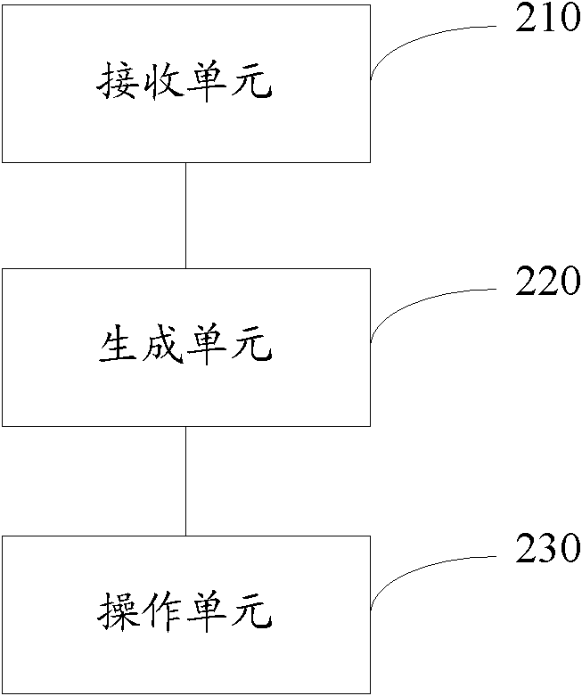
[0051] Hereinafter, the implementation of the method and device for FPGA to communicate with DSP through the DDR2 interface in the embodiment of the present invention will be described in detail in conjunction with the accompanying drawings.

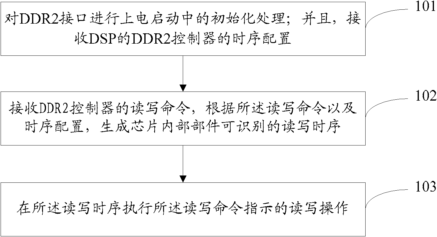
[0052] figure 1 For the embodiment of the present invention FPGA communicates with the method flow diagram of DSP through DDR2 interface, this method can be applicable to in the FPGA chip; figure 1 As shown, the method includes:

[0053] Step 101: The FPGA performs initialization processing on the DDR2 interface during power-on startup; and receives the timing configuration of the DDR2 controller of the DSP;

[0054] Wherein, the initialization process may include:

[0055] A: Receive the initialization command of the mode register (MR) and the initialization command of the extended mode register (EMR) from the DDR2 of the DSP;

[0056] MR includes parameters such as CAS latency (CL), trigger type, and trigger length (BL).

[0057] E...


PUM


Abstract

The invention discloses a method and device for an FPGA (field programmable gate array) to communicate with a DSP (digital signal processor) via a DDR2 (double data rate 2) interface. The method comprises: initializing the DDR2 interface in the electric starting process; receiving timing sequence configuration of a DDR2 controller of the DSP; generating a reading and writing timing sequence according to reading and writing instructions and the timing sequence configuration when receiving the reading and writing instructions sent by the DDR2 controller; and performing reading and writing operations indicated by the reading and writing instructions at the reading and writing timing sequence. By utilizing the method and the device, the FPGA is enabled to communicate with the DSP via the DDR2 interface, thus the cost and resource consumption of the FPGA chip devices communicating with the DSP are reduced.

Description

technical field [0001] The present invention relates to the communication field, in particular to a method and a device for communicating with a Field Programmable Gate Array (FPGA, Field Programmable Gate Array) and a Digital Signal Processor (DSP, Digital Signal Processor) through a DDR2 interface. Background technique [0002] With the development of DSP technology and the increase of digital processing bandwidth, the current DSP external interface is developing towards high-speed serial interface, and the original parallel low-speed interface is abandoned, which is beneficial to reduce the number of pins of the chip, thereby reducing the size of the chip. The size also greatly simplifies the complexity of PCB wiring. [0003] But the ensuing problem is: the use of high-speed serial bus has brought a substantial increase in device costs, including the chip itself and the chip connected to it, such as FPGA. When FPGA uses high-speed serial bus and DSP link, it must use a b...

Claims


Application Information

Patent Timeline
IPC IPC(8): G06F13/38
Inventor 何梁
Owner WUHAN HONGXIN TELECOMM TECH CO LTD
Learn More