Radio frequency (RF) test method for semiconductor RF device

A technology of radio frequency testing and radio frequency devices, which is applied in the field of radio frequency testing of semiconductor radio frequency devices, can solve the problems of reducing the accuracy of radio frequency testing of semiconductor radio frequency devices, and achieve the effect of overcoming parasitic effects and improving accuracy

Inactive Publication Date: 2011-05-18
SHANGHAI HUA HONG NEC ELECTRONICS
View PDF0 Cites 6 Cited by
  • Summary
  • Abstract
  • Description
  • Claims
  • Application Information

AI Technical Summary

Problems solved by technology

However, the traditional method of specially designing some de-embedding structures inevitably adds redundant parasitic structures to the layout in order to achieve grounding effects, which will have adverse parasitic effects on the accuracy of the measured RF parameters of the overall RF test structure. Resulting in a reduction in the accuracy of RF testing of semiconductor RF devices

Method used


Image

  • Radio frequency (RF) test method for semiconductor RF device
  • Radio frequency (RF) test method for semiconductor RF device
  • Radio frequency (RF) test method for semiconductor RF device

Examples


Embodiment Construction

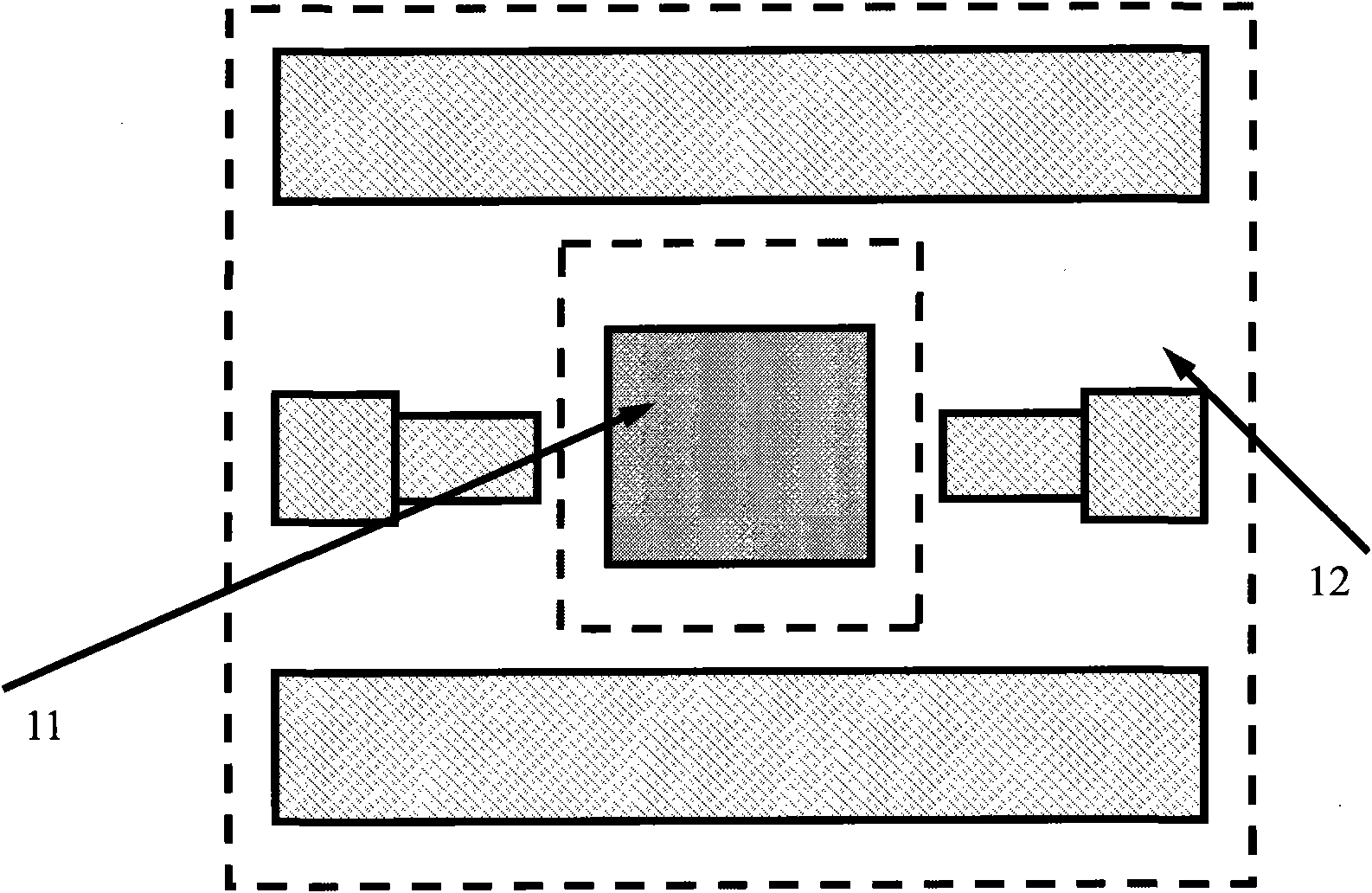
[0013] The overall RF test structure used in the RF integrated circuit process to test semiconductor RF devices is as follows: figure 1 As shown, it includes two parts: a semiconductor radio frequency device structure 11 to be tested and a de-embedding structure 12 designed for placement of radio frequency probes. The accurate radio frequency parameters of the semiconductor radio frequency device should be the measured radio frequency parameters of the overall radio frequency test structure minus the influence of the radio frequency parameters of the de-embedding structure.

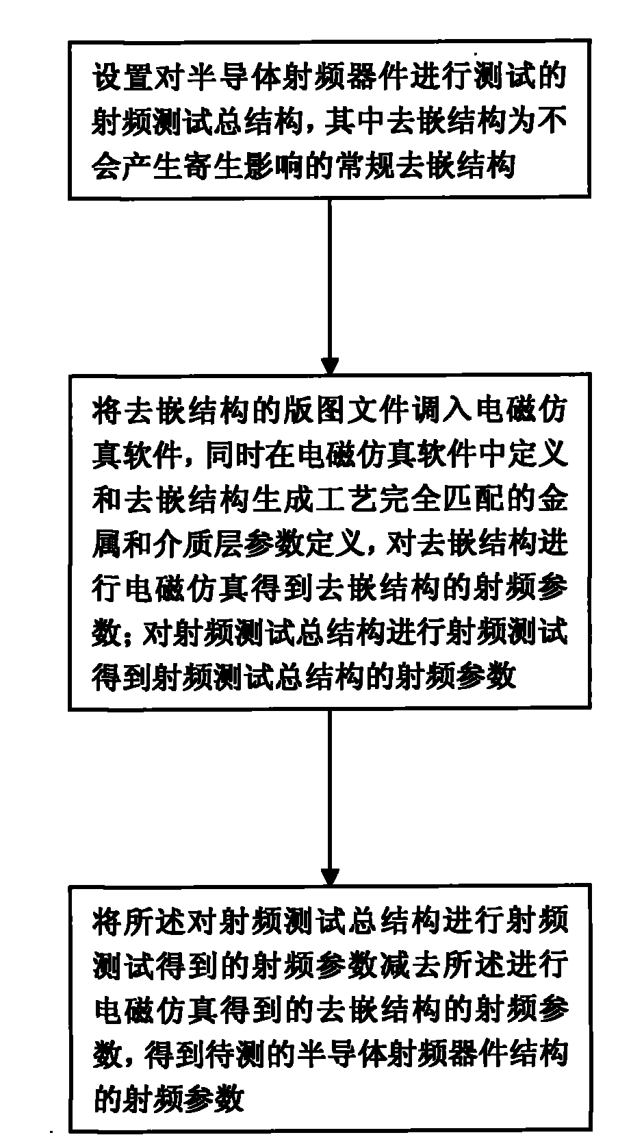
[0014] The flow chart of an embodiment of the radio frequency testing method of the semiconductor radio frequency device of the present invention is as follows figure 2 shown, including the following steps:

[0015] One. the general structure of the radio frequency test that semiconductor radio frequency device is tested comprises two parts: the semiconductor radio frequency device structure to be teste...


PUM


Abstract

The invention discloses a radio frequency (RF) test method for a semiconductor RF device. The RF test method for the semiconductor RF device comprises the following steps of: setting an RF test total structure for testing the semiconductor RF device, wherein the RF test total structure comprises a semiconductor RF device structure to be tested and a de-embedding structure designed for placing an RF probe; calling a layout file of the de-embedding structure into electromagnetic simulation software and performing electromagnetic simulation on the de-embedding structure to acquire an RF parameter of the de-embedding structure; performing the RF test on the RF test total structure to acquire an RF parameter of the RF test total structure; and subtracting the RF parameter of the de-embedding structure by using the RF parameter of the RF test total structure to acquire an RF parameter of the semiconductor RF device structure to be tested. By the RF test method for the semiconductor RF device, the accuracy of the RF parameter is high, wherein the RF parameter is acquired by that the RF test total structure for testing the semiconductor RF device tests the semiconductor RF device by utilizing the conventional de-embedding structure which does not generate parasitic influence.

Description

technical field [0001] The invention relates to semiconductor testing technology, in particular to a radio frequency testing method of a semiconductor radio frequency device. Background technique [0002] The overall RF test structure used in the RF integrated circuit process to test semiconductor RF devices is as follows: figure 1 As shown, it includes two parts: a semiconductor radio frequency device structure 11 to be tested and a de-embedding structure 12 designed for placement of radio frequency probes. The accurate radio frequency parameters of the semiconductor radio frequency device should be the measured radio frequency parameters of the overall radio frequency test structure minus the influence of the radio frequency parameters of the de-embedded structure. The traditional method is to specially design some de-embedding structures and perform corresponding de-embedding operations in the layout design, so as to eliminate the influence of the de-embedding structures...

Claims


Application Information

Patent Timeline
Patent Type & Authority Applications(China)
IPC IPC(8): G01R31/26
Inventor 周天舒
Owner SHANGHAI HUA HONG NEC ELECTRONICS
Why Eureka
Try Eureka