Optical imaging touch sensing system and imaging method

A technology of touch sensing and optical imaging, applied in the direction of instruments, electrical digital data processing, and input/output process of data processing, etc., can solve problems such as difficulty in reducing production costs, hindering the promotion of image sensing devices for touch screens, and complex optical paths , to achieve the effects of reducing optical equipment and hardware equipment, optimizing image processing methods, and simplifying the optical path structure

Active Publication Date: 2011-05-18
RETURNSTAR INTERACTIVE TECH GRP
View PDF3 Cites 13 Cited by
  • Summary
  • Abstract
  • Description
  • Claims
  • Application Information

AI Technical Summary

Problems solved by technology

Due to the poor anti-interference of the current touch screen image sensing device, the optical path is complicated, a large number of optical equipment, and complex hardware equipment are required, so it is difficult to reduce the production cost, which hinders the popularization of the touch screen image sensing device

Method used


Image

  • Optical imaging touch sensing system and imaging method
  • Optical imaging touch sensing system and imaging method
  • Optical imaging touch sensing system and imaging method

Examples


Embodiment Construction

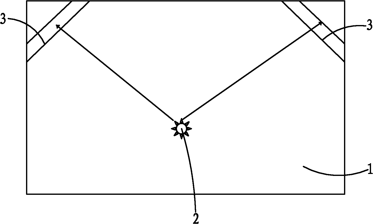
[0015] Such as figure 1 As shown, the optical path diagram of the optical imaging touch sensing system includes a touch screen 1, an infrared electronic pen 2, and an image processing circuit; the image processing circuit includes two imaging sensor devices, and the two imaging sensor devices are respectively installed on both sides of the touch screen 1 ; The imaging sensor device includes an optical lens 3 with a filter for visible light. The optical path structure in the present invention adopts a luminous pen and a filter to form a binocular vision system, and the filter is used to filter out visible light and pass through the luminous pen, which is different from the prior art in that it passes through visible light and filters out Infrared light does the opposite.

[0016] When the infrared electronic pen 2 touches the touch screen 1, the light touch switch inside the infrared electronic pen 2 is turned on, and the infrared electronic pen 2 can emit 800-1600nm infrared ...


PUM


Abstract

The invention relates to an optical imaging touch sensing system comprising a touch screen, an infrared electronic pen and an image processing circuit, wherein the image processing circuit comprises two imaging sensing elements, the two imaging sensing elements are respectively arranged at two sides of the touch screen, and each imaging sensing element comprises a belt filter visible light optical lens. Bright spot images are formed on the imaging sensing elements arranged at two sides of the touch screen by invisible infrared rays emitted from the infrared electronic pen via a filter lens when the infrared electronic pen moves on the touch screen, the images are computed via the image processing circuit to resolve a two-dimensional coordinate of the infrared emitting pen on the touch screen, and finally, coordinate data are sent to a computer via a USB (Universal Serial Bus) interface, and positional information conversion from the infrared emitting pen to a computer mouse is realized through a computer positioning program. By virtue of the invention, the optical path structure of a sensor is simplified, the numbers of optical devices and hardware devices are reduced, meanwhile, an image processing mode is optimized by a special algorithm, and the anti-interference performance of the system is enhanced.

Description

【Technical field】 [0001] The invention relates to an optical imaging touch sensing system for an infrared touch screen and an imaging method thereof, belonging to the field of optics and imaging technology, in particular to the field of imaging technology for touch screens and electronic whiteboards using image sensing for positioning. 【Background technique】 [0002] With the popularization of touch screens, image sensing devices of touch screens are also widely used, which include image sensors composed of image sensing chips and optical imaging systems, and are installed on the edge of the screen to be detected. It uses an area array or line array image sensor, which includes a two-way optical imaging system composed of a convex-concave lens and necessary mirrors. The two lenses are separated from each other and face the screen, thereby utilizing the function of stereoscopic photography Realize the positioning of the touch object. The two-way optical imaging system uses i...

Claims


Application Information

Patent Timeline
Patent Type & Authority Applications(China)
IPC IPC(8): G06F3/042
Inventor 丁万年陈日良陈丽洪文杰
Owner RETURNSTAR INTERACTIVE TECH GRP
Why Eureka
Try Eureka