
Linear source follower

A technology of follower and linear source, applied to amplifiers with impedance circuits, etc., can solve problems such as linearity deterioration

Active Publication Date: 2011-05-25
TSINGHUA UNIV
View PDF3 Cites 7 Cited by
  • Summary
  • Abstract
  • Description
  • Claims
  • Application Information

AI Technical Summary

Problems solved by technology

Although the implementation is very simple, there are some disadvantages
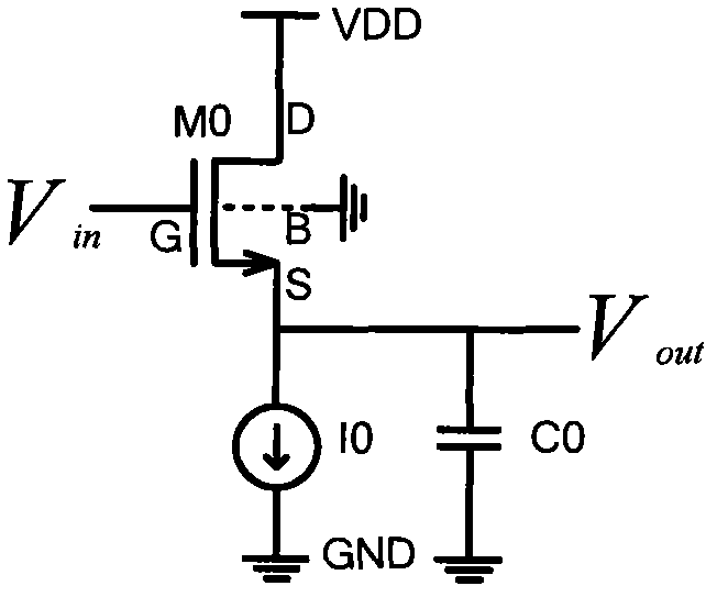
When the input signal V in When changing, the voltage difference between the drain D and the source S of the transistor M0, the voltage difference between the source S and the substrate B all change with the change of the input signal, and the body effect, channel length modulation effect, etc. Limits the linearity of conventional source followers
When the output signal changes with the input signal, the transistor M0 needs to charge the load C0, so the current flowing through the transistor M0 changes, further deteriorating the linearity

Method used


Image

  • Linear source follower
  • Linear source follower
  • Linear source follower

Examples


Embodiment Construction

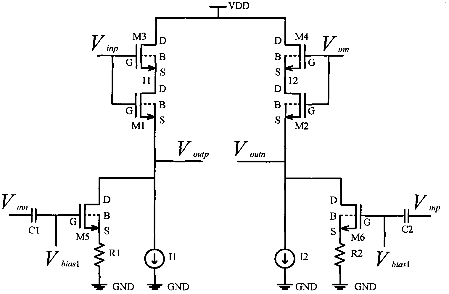
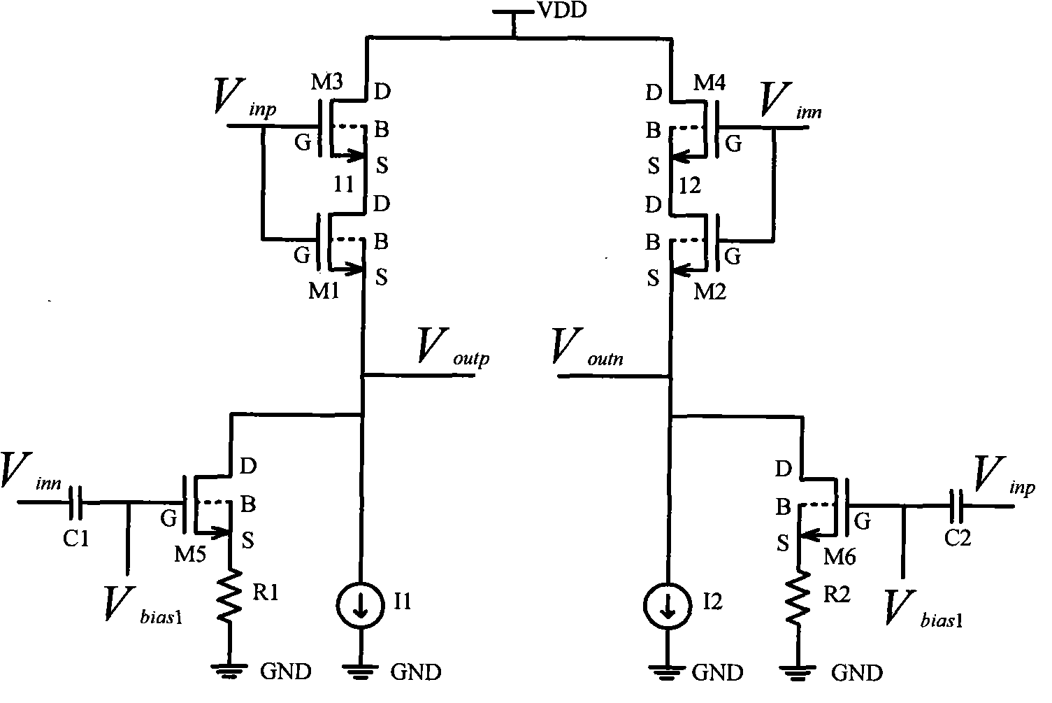
[0019] The third N-type field effect transistor M3, the gate is connected to the input voltage V inp , the drain is connected to the power supply VDD, the substrate is connected to the source, the third N-type field effect transistor M3 always works in the saturation region, and the gate of the first N-type field effect transistor M1 is connected to the input voltage V inp , the source of the third N-type field effect transistor M3 is connected to the drain of the first N-type field effect transistor M1;

[0020] The fourth N-type field effect transistor M4, the gate is connected to the input voltage V inn , the drain is connected to the power supply VDD, the substrate is connected to the source, the fourth N-type field effect transistor M4 always works in the saturation region, and the gate of the second N-type field effect transistor M2 is connected to the input voltage V inn , the source of the fourth N-type field effect transistor M4 is connected to the drain of the secon...


PUM


Abstract

The invention discloses a linear source follower, which belongs to the technical field of voltage followers and is characterized in that: transistors M1 and M3 are arranged in a cascade mode, and the grids of the transistors M1 and M3 are both connected with an input Vinp; transistors M2 and M4 are connected in a cascade mode, and the grids of the transistors M2 and M4 are both connected with aninput Vinn; the transistors M3 and M4 are both low-threshold transistors; and the transistors M1 and M2 are both high-threshold transistors. The sources S of the transistors M1, M2, M3 and M4 are allconnected with a substrate B. The grid of a transistor M5 is connected with a bias voltage Vbias1 and is connected with the input signal Vinn through a capacitor C1, the drain of the transistor M5 isconnected with an output Voutp, and the source of the transistor M5 is grounded through a resistor R1. The grid of a transistor M6 is connected with the bias voltage Vbias1 and is connected with an input signal Vinp through a capacitor C2, the drain of the transistor M6 is connected with an output Voutn, and the source of the transistor M6 is grounded through a resistor R2. In the invention, a channel length modulation effect and a bulk effect are eliminated, the change of a bias current is lowered, and the linear source follower has the advantages of high linearity under a high-speed input signal.

Description

technical field [0001] The invention belongs to the design of ultra-large-scale integrated circuits in the fields of microelectronics and solid-state electronics, and relates to a novel source follower circuit, which can be widely used in the fields of analog integrated circuit design and integrated circuit testing. Background technique [0002] This invention relates to the design of high performance analog integrated circuits such as high speed analog to digital converters. Voltage follower is one of the most important modules in analog circuits and is widely used in analog integrated circuit design. It is generally required that the voltage follower has high linearity for any input signal, so that the output is as close as possible to the input. [0003] A conventional source follower such as figure 1 shown. Although very simple to implement, there are some drawbacks. When the input signal V in When changing, the voltage difference between the drain D and the source ...

Claims


Application Information

Patent Timeline
IPC IPC(8): H03F3/50
Inventor 魏琦陈夏阳杨华中
Owner TSINGHUA UNIV
Learn More