CMOS input signal buffer applied to front end of high-speed ADC

An input buffer, input signal technology, applied in the direction of logic circuit coupling/interface, analog-to-digital converter, electrical components, etc. using field effect transistors, which can solve the comparison result error, comparator input common mode drift, source follower output common mode level drift and other issues

Pending Publication Date: 2020-10-09
FUDAN UNIV
View PDF0 Cites 4 Cited by
  • Summary
  • Abstract
  • Description
  • Claims
  • Application Information

AI Technical Summary

Problems solved by technology

[0004] A common input signal buffer adopts an open-loop source follower structure. The source follower of the open-loop structure can obtain larger bandwidth, higher linearity, low output impedance, and larger signal drive capability. However, du...

Method used


Image

  • CMOS input signal buffer applied to front end of high-speed ADC
  • CMOS input signal buffer applied to front end of high-speed ADC
  • CMOS input signal buffer applied to front end of high-speed ADC

Examples


Embodiment Construction

[0021] Hereinafter, the present invention will be described in more detail with reference to the accompanying drawings. In the various figures, identical elements are indicated with similar reference numerals. For the sake of clarity, various parts in the drawings have not been drawn to scale. Also, some well-known parts may not be shown in the drawings.

[0022] In the following, many specific details of the present invention are described, such as device structures, materials, dimensions, processing techniques and techniques, for a clearer understanding of the present invention. However, the invention may be practiced without these specific details, as will be understood by those skilled in the art.

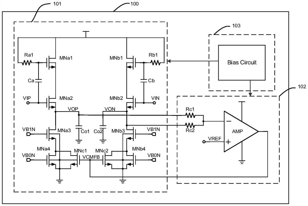
[0023] figure 1 A schematic diagram of an input signal buffer circuit with a common-mode feedback circuit is shown.

[0024] like figure 1 As shown, the input signal buffer circuit includes a differential source follower type input buffer module 101 , a common-mode voltage...


PUM


Abstract

The invention belongs to the technical field of integrated circuits, and particularly relates to a CMOS input signal buffer applied to the front end of a high-speed ADC. The circuit structure comprises an input buffer with two differential source following structures, a common-mode feedback circuit module and a bias circuit module. According to the invention, stable common-mode output of a sourcefollower can be ensured; a channel length modulation effect under a deep submicron CMOS process is avoided; a N-type transistor adopts a deep N-well device to eliminate the substrate bias modulation effect. A cascode current source with large output impedance is used for providing bias current for an input transistor so as to relieve output signal nonlinearity caused by input signal changes. The buffer is used in an ADC circuit, can play a role in improving linearity and isolating an input signal from a post-stage circuit, has good linearity even when an input signal with higher frequency is input, and is particularly suitable for a front-end buffer circuit of a high-speed ADC.

Description

technical field [0001] The invention belongs to the technical field of integrated circuits, and in particular relates to a CMOS input signal buffer applied to the front end of a high-speed ADC. Background technique [0002] Analog-to-digital converter (ADC) is a bridge connecting the analog world and the digital world. Physical signals in nature such as force, temperature, light, sound, etc. are all analog signals. However, digital signal processing has higher reliability and Lower cost, so the analog signal needs to be converted to digital first. Therefore, the analog-to-digital converter is a key component in many analog-to-digital hybrid systems, and becomes one of the important factors restricting the performance of the entire system. With the gradual development of the fifth-generation wireless communication technology, various application scenarios such as the Internet of Everything and 5G communication micro base stations have brought new challenges to the design of ...

Claims


Application Information

Patent Timeline
IPC IPC(8): H03K19/0185H03M1/12
CPCH03K19/0185H03M1/129
Inventor 马顺利魏继鹏李满鑫任俊彦
Owner FUDAN UNIV
Why Eureka
Try Eureka